The purpose of this paper is to understand the process of DFT to be performed on a particular design using the SYNOPSYS tool set. Verification of which can be done at the end by the count of number of DRC’s (Design Rule Check) violations in the process. All the faults should be checked to get the fault free design based on the theoretical background available. The process is then followed on the SYNOPSYS tools for the removal of faults and also for the verification of the same.
Keywords |
| DRC, Scan Insertion, Fault Checking. |
INTRODUCTION |
| ASIC design also known as Application Specific Integrated Circuit. It is a semi-custom/full custom design methodology
where already available standard library cells are utilized for the design of customized applications when time to market is
an important criteria. Whereas for optimized designs everything is designed from the RTL coding stage. The entire ASIC
design flow is divided into three main parts namely, design, synthesis, and place & route. At the end of successful
completion of all three steps the layout gets ready for physical implementation. But along with these stages there is also a
stage called DFT (Design for test), DFT is increasingly gaining momentum among ASIC Design Engineers. This
techniques provide measures to comprehensively test the manufactured device for the quality and coverage. |
TYPES OF DFT |
| The main DFT techniques that are currently in use today are: Scan Insertion, memory BIST Insertion, Logic BIST Insertion
and Boundary – Scan Insertion. Of all four, Scan and Logic BIST insertion is the most complex and challenging technique,
since it involves various design issues that need to be resolved, in order to get full coverage of the design. Here, we will
mainly focus on Scan Insertion technique for the DFT Process. JTAG or boundary scan is primarily used for testing the
board connections, without unplugging the chip from the board. |
| Scan is one of the most widespread DFT techniques used by design engineers to test the chip for defects such as stuck-at
faults. It is possible to attain a very high percent fault coverage (usually above 95%) for most of the designs. |
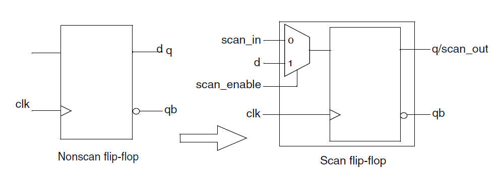
| The scan insertion technique involves replacing all the flip-flops in the design, with special flops that contain built-in logic,
solely for testability. The most prevalently used architecture is the multiplexed flip-flop. This type of architecture incorporates
a 2-input mux at the input of the D-type flip-flop. The select line of the mux determines the mode of the device, i.e. it enables
the mux to be either in the normal operational mode (functional mode with normal data going in) or in the test mode (with
scanned data going in).These scan-flops are linked together (using the scan-data input of the mux) to form a scan-chain, that
functions like a serial shift register. During scan mode, a combination of patterns are applied to the primary input, and shifted
out through the scan-chain. If done correctly, this technique provides a very high coverage for all the combinational and
sequential logic with in a chip. Figure – 1 shows the difference between Non scan and Scan Flip-Flop that are incorporated in the
design. |
| Other architectures available along with multiplexed type flip-flops are the lssd structure, clocked scan structure etc.
As mentioned above, the most commonly used architecture is the multiplexed flip-flop. For this reason, throughout this paper
the focus remains on the multiplexed flip-flop type architecture, for DFT scan insertion. |
| Scan can also be used to test the DUT for any possible timing violations. In order to understand this, we need to dig
deeper into the operation of scan technique. Basically, scan uses two cycles: Capture and Shift. Scan data is injected from the
primary inputs into the device where it is captured by the flops (going through logic) and is then shifted out to primary outputs
where it is compared against the expected results. The signal that selects between the capture and shift cycle is usually called
the scan_enable signal. In addition another signal is also used which is usually called the scan_mode signal. Scan mode
signal is used to put the DUT in test conditions. In general, designs are modified such that under test conditions the device
behaves different as opposed to the normal functional behavior. This modification is desired in order to achieve greater
control and/or observability. Sometimes it is done simply to comply with the strict DFT rules. |
| The following list summarizes the basic scan operation: |
| Load/Unload scan chain (shift cycle) |
| Force primary inputs (except clocks) |
| Measure primary outputs |
| Pulse clock to capture functional data (capture cycle) |
| In order to understand how scan can be used to test the device for timing, a basic understanding of shift and capture cycle is
necessary. |
DFT PROCESS |
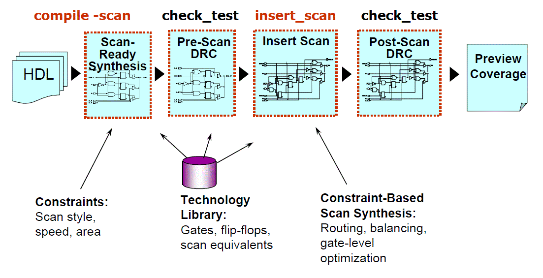
| The Overview of DFT Compiles flow is shown in the Figure – 2. The flow is as follows. |
| • Firstly the specifications of the design are decided, and the micro – architecture for the same is created for further
use. |
| • RTL coding for the design is done with the reference of micro – architecture created earlier, timing constraints for
the same are designed. |
| • RTL code and the constraints are feed to the compiler along with the target, link and symbol library for the
generation of the netlist. (here we used lsi_10k as libraries) |
| • Look out for the Tri-State errors. If you encounter any of such errors, change the code by bypassing the memory
elements but make sure that the functionality of the code should not change. This would help to reduce many of
the errors during the DFT_DRC check. |
| • Generate the netlist from the designed RTL code and the constraints. |
| • Compile the design and check for the timing violation if any, after which proceed with the setting of the DFT
signals in the design like Scan_in, Scan_out and Scan_en. |
| • Insert the Scan chains in the design by the command |
| • set_scan_configuration -chain_count #No. -create_dedicated_scan_out_ports true |
| • Here, #No. determines the total number of chains that you want to insert in the design. |
| • Note: - single chain should contain maximum of 10 Flip-Flops of the design for the better operation on the
same. |
| • Create the test protocol of the design and perform the dft_drc check on the design. |
| • Now check for if any violations in the design, if not proceed with the insertion of dft in the design by |
| • insert_dft |
| • Write the protocol in desired folder to use it further for the process of ATPG (Automatic Test Pattern Generation),
to check for the proper functioning of the design. |
RESULTS |
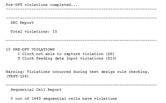
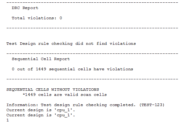
| We had performed the DFT on MIPS Multi-cycle Processor and the OpenSPARC T1 Processor, results for the
same are as shown below. |
| As shown in Figure – 6 we had observed the tri-state error in the OpenSPARC T1 processor and the same was
overcome by editing the memory code wherein we bypassed the memory elements used at the same time without changing
the functionality of the design. |
CONCLUSION |
| DFT techniques are essential to an efficient and success fault testing of the manufactured device. By implementing
DFT features early in the design cycle, full test coverage on the design may be achieved, thereby reducing the debugging
time normally spent at the tester after the device is fabricated. This paper described the basic testability techniques that are
currently in use. A detailed description was provided for the scan insertion DFT technique, using the DFT Compiler. Various
guidelines and solutions were also provided that may help the user to identify the issues and problems related to this
technique. |
Figures at a glance |
 |
 |
 |
| Figure 1 |
Figure 2 |
Figure 3 |
|
 |
 |
 |
| Figure 4 |
Figure 5 |
Figure 6 |
|
References |
- Core architecture of MIPS Multi â cycle processor: David A. Patterson and John L. Hennessy, Computer Organization and Design â The Hardware and Software Interface, 3rd Edition.
- Implementation and Design Planning: Synopsys, DFT compiler User Guide, Version C-2009.06, July 2009.
- Video LectureâÂÂs: Prof. I Sengupta â IIT Kharagpur, YouTube.
- Overview of DFT Compiler Flow by Synopsys
|