International Journal of Innovative Research in Science, Engineering and Technology
ISSN ONLINE(2319-8753)PRINT(2347-6710)
ISSN ONLINE(2319-8753)PRINT(2347-6710)
Seemadevi B. Patil, Kureshi Abdul Kadir
|
| Related article at Pubmed, Scholar Google |
Visit for more related articles at International Journal of Innovative Research in Science, Engineering and Technology
This paper presents the review of the thermal noise in CMOS devices. The various methods discussed takes into account the modelling of the CMOS devices for the thermal noise. The paper discusses the resistor model, gradual channel approximation, induced gate thermal noise, noise contribution by Rs and Rd. These models can be used for long channel and short channel device modelling by taking into account all of the above models. The thermal noise behaviour of MOSFET with decreasing channel length can be understood.
Keywords |
| thermal noise, excess noise, scaling, CMOS, GCA |
INTRODUCTION |
| For continuous downscaling of CMOS devices for RF applications accurate modelling of CMOS becomes an important aspect to optimize the circuit performance and development time required. However, while working at high frequencies and high speed circuits the thermal noise becomes a critical issue preventing these circuits from their designed performance. |
| MOSFETs behave basically as voltage-controlled resistors. Therefore, thermal noise is present in MOSFETs, which is the result of random potential fluctuations in the channel. These fluctuations in the channel lead to one source of thermal noise, which is the drain current noise In addition fluctuations are introduced through the oxide capacitance of the gate terminal, into the gate and cause a gate noise current known as induced gate thermal noise. The drain current noise and the gate noise are correlated because they both are agitated by the thermal noise sources in the channel Since noise characteristics are one of the main concerns in the LNA design, it is very important for circuit designers to be able to predict and calculate the noise of MOS devices with reasonable accuracy and also to recognize the noise dependence on the geometry and biasing conditions of the device |
NOISE MODELS FOR THERMAL NOISE |
| The fundamental assumption for most analytical and semi analytical MOSFET thermal noise models is gradual channel approximation (GCA). For the ideal two-terminal MOS device as shown in figure 1 the channel potential is a gradually changing function of position along the channel from the drain to the source, which varies very little along the channel over a distance of the order of the gate oxide insulator thickness. |
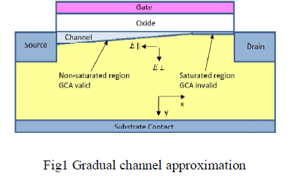 |
| The GCA is valid for long channel MOSFET where the aspect ratio between the gate length and the vertical distance of space charge region from the gate electrode is large. Under assumption of this model some of the noise models were developed, The model given by Klaassen and Prins[1] based on the relationship between channel current and local channel conductivity of the MOSFET is widely used to calculate the conductivity of the long channel MOSFET the drain current Id is expressed as |
 |
| where V(x) is the channel potential at x and dV(x)/dx is dc voltage difference in the electron quasi-Fermi level in the inversion layer and hole quasi-Fermi level in the substrate at position at x and g the local channel conductivity. For a simple long channel MOSFET the |
 |
| where Vod is the overdrive voltage and it equals Vgs- Vth. V(x) is the channel potential at 0, W is the width of the MOSFET, μ is the mobility, and Cox is the oxide capa citance per unit area. Assuming a differential segment Δx of the channel, a small noise voltage contribution V(x) across the segment Δx is observed, which is added to the dc voltage V(x). This voltage can cause noise in the drain current, which leads to a change in the dc current through the MOSFET. The power spectral density of thermal noise of a long-channel MOSFET is |
| One more model that takes into account the electron effects that is given by Albert van der Ziel[] in his model by substituting the lattice temperature with carrier temperature Te(x) and modified the above model as given below |
 |
| When Te(x) is known then ������ can be easily calculated. |
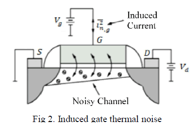
| In addition, a MOSFET can be described as an RC network at high frequencies, with the oxide capacitance of the gate terminal and the resistance due to the channel itself. The fluctuations in the channel are introduced to the gate and cause a gate noise current which is shown in figure 2 also known as induced gate thermal noise |
 |
| The induced gate noise can be expressed as |
| Where β is independent of substrate conductivity and its value is 4/3 in saturation region for long channel MOSFET the conductance has the form of gg |
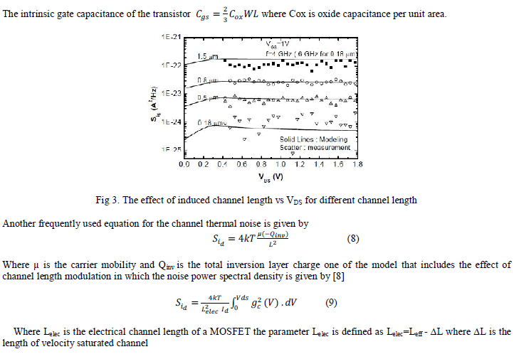 |
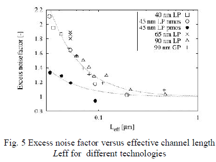
| In sub-100-nm technologies, however, microscopic excess noise starts to play a significant role and its incorporation in thermal noise models is unavoidable. It could be expected that they would increase sharply when entering the sub-100-nm regime, where channel length scales down much more rapidly than supply voltage, resulting in large lateral electric fields. Indeed, larger deviations from pure thermal noise have been experimentally observed in sub-100-nm channels |
| The various effects that need to be accounted for the short channel length are given as below |
| A. Velocity Saturation |
| The electron transport in MOSFET is affected by the velocity saturation effect and is proportional to α power of applied power of applied gate voltage. Thus the saturation current is affected by the velocity saturation effect and could be described by using the α power-law MOSFET model [6] |
| B. Channel Length modulation |
| The effect of CLM enters equation (4) only through L2 Ids in the prefactor. Because Ids is roughly proportional to 1/L,the effect of CLM on Sid is very similar to its effect on Ids. Because CLM has no impact on the value of gds0, the effectof CLM in saturation is that γ is somewhat increased beyond its long-channel value 2/3.[3] |
| C. GATE resistance |
| A gate resistance Rg generates a noise voltage Sv=4kBTRg Which transfers to the drain current via transconductance gm adding contribution |
 |
| to the drain current noise |
| D. Substrate Resistance |
| The contribution to the drain current noise is given by |
| Rb gives rise to induced substrate noise. The effect of substrate resistance is on the drain current noise is small provided that the MOSFET is designed with low substrate resistance[3] |
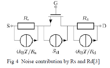 |
| The impact of source and drain resistance on noise is less but may be very significant. A straightforward small-signal analysis of the circuit shown in Fig. 4 gives that |
| Where |
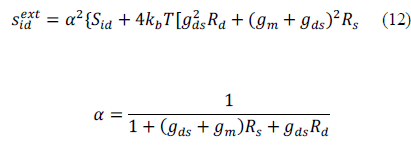 |
| It is expected that a correction is required in the presence of large (lateral) electric fields. Such fields occur in advanced CMOS technologies, where the channel length is scaled down faster than the supply voltage (as typically happens for 100- nm technologies and beyond). Therefore a model is needed that captures the onset of nonequilibrium transport and its effect on thermal noise. This noise which is called as excess noise [9]should also be taken into consideration The results obtained with the above model without taking into consideration the effect of excess noise are as shown in the figure. |
 |
CONCLUSION |
| Here the various models which take into consideration modelling of thermal noise for the long channel devices are discussed. Also thermal noise modelling of short-channel devices can be established by taking consideration of short channel effects including velocity saturation and channel-length modulation. The importance of accounting for all intrinsic and parasitic noise sources in the MOS device can be emphasized. The inclusion of microscopic excess noise in noise models is also studied. The various discussed models can be implemented in circuit simulators for RF circuit design and can be very helpful in predicting circuit noise performance. |
References |
|