International Journal of Innovative Research in Science, Engineering and Technology
ISSN ONLINE(2319-8753)PRINT(2347-6710)
ISSN ONLINE(2319-8753)PRINT(2347-6710)
Yogesh S. Watile1, A. S. Khobragade2
|
| Related article at Pubmed, Scholar Google |
Visit for more related articles at International Journal of Innovative Research in Science, Engineering and Technology
We report on the design of efficient cache controller suitable for use in FPGA-based processors. Semiconductor memory which can operate at speeds comparable with the operation of the processor exists; it is not economical to provide all the main memory with very high speed semiconductor memory. The problem can be alleviated by introducing a small block of high speed memory called a cache between the main memory and the processor. Set-associative mapping compromise between a fully associative cache and a direct mapped cache, as it increases speed. With reference to set associative cache memory we have designed cache controller. Spatial locality of reference is used for tracking cache miss induced in cache memory. In order to increase speed , less power consumption and tracking of cache miss in 4-way set associative cache memory, FPGA cache controller will proposed by this research work . We believe that our design work achieves less circuit complexity, less power consumption and high speed in terms of FPGA resource usage
Keywords |
| Cache Tag memory, Cache controller, Counter, Cache Tag comparator, Cache data memory. |
INTRODUCTION |
| Field-programmable gate arrays (FPGAs) have recently been garnering attention for their successful use in computing applications. Indeed, recent work has shown that implementing computations using FPGA hardware has the potential to bring orders of magnitude improvement in energy-efficiency and throughput vs. realizing computations in software running on a conventional processor. While a variety of different memory architectures are possible in processor/accelerator systems, a commonly-used approach is one where data shared between the processor and accelerators resides in a shared memory hierarchy comprised of a cache and main memory. The advantage of such a model is its simplicity, as cache coherency mechanisms are not required despite this potential limitation; we use the shared memory model as the basis of our initial investigation, with our results being applicable (in future) multi-cache scenarios[1]. In our work, data shared among the processor and parallel accelerators is to accessed through a shared L1 cache, implemented using on-FPGA memory. Processors are generally able to perform operations on operands faster than the access time of large capacity main memory. Though semiconductor memory which can operate at speeds comparable with the operation of the processor exists, it is not economical to provide all the main memory with very high speed semiconductor memory. The problem can be alleviated by introducing a small block of high speed memory called a cache between the main memory and the processor. Cache systems are on-chip memory element used to store data. In the direct scheme, all words stored in the cache must have different indices. The tags may be the same or different. In the fully associative scheme, blocks can displace any other block and can be placed anywhere, but the cost of the fully associative memories operate relatively slowly. Set-associative mapping allows a limited number of blocks, with the same index and different tags, in the cache and can therefore be considered as a compromise between a fully associative cache and a direct mapped cache. cache controller is used for tracking induced miss rate in cache memory. Any data requested by microprocessor is present in cache memory then the term is called „cache hitâÂÂ. The advantage of storing data on cache, as compared to RAM, is that it has faster retrieval times, but it has disadvantage of on-chip energy consumption. This paper deals with the design of efficient cache memory for detecting miss rate in cache memory and less power consumption. This cache memory may used in future work to design FPGA based cache controller. |
II.SYSTEM ARCHITECTURE OVERVIEW |
| Cache controller that communicates between microprocessor and cache memory to carry out memory related operations. The functionality of the design is explained below. Cache controller receive address that microprocessor wants to access Cache controller looks for the address in L1 cache. If address present in L1 cache the data from location is provided to microprocessor via data bus. If the address not found in L1 cache then cache miss will occur. Cache controller then looks same address in cache L2. If address present in L2 cache the data from location is provided to microprocessor. The same data will replace in cache L1. If the address not found in L2 cache then cache miss will occur. |
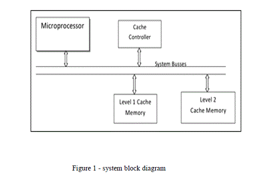 |
| In our paper work we designed 4-way set associative cache memory(L1) for detecting miss rate in cache memory and less power consumption and To track cache miss in cache memory we designed cache controller .This work will be used in design of FPGA based processor. |
III. DESIGNED WORK |
| In our designed work, we designed 4-way set associative cache memory L1 using FPGA as 4-way set associative cache strike a good balance between lower miss rate and higher cost [5]. Our paper work deal with the design of 4-way set associative cache memory for the detection of cache misses and design of cache controller for tracking induced cache misses. Cache memory designed consists of cache tag memory, cache tag comparator, counter, cache data memory and address field separator. Address Requested by microprocessor is compared with addresses of data in main memory which are stored in tag memory with the help of cache tag comparator. If requested address is found in cache Tag memory then cache hit will occur and corresponding data related to requested address stored in a data memory is given to the microprocessor. If requested address is not found in cache Tag memory then cache miss will occur. To reduced cache miss we designed cache controller. Once requested address is missing then cache controller generate the address range. This address range is nothing but the neighboring addresses of miss requested address. This address rang given to the microprocessor by cache controller to replace addresses in this range to the cache tag memory. This will reduce the cache misses. |
IV. CACHE MEMORY |
| Cache systems are on-chip memory element used to store data. Cache memory is used to increase the data transfer rate between processor and main memory. 4-way set associative Cache memory consist of the following modules 1)Cache tag memory,2) cache data memory,3) cache tag comparator, 4)address field separator and 5) counter. A.cache tag memory The cache tag memory stored address of data in main memory. Cache tag memory is modelled using behavioural style of modelling in VHDL (for example: 22-bit cache tag memory). Figure 2 shows the diagram of cache tag memory of 22 bit. To design 4-way set associative cache memory of 1KB, we need 4 ways of such 256 bytes of Tag memory and data memory. When „weâÂÂ=1 it performs writing operation and „weâÂÂ=0 it performs reading operation. |
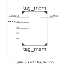 |
| Data stored in the tag memory will be addresses of main memory. When microprocessor requests an address, it will compare with the data stored in the Cache Tag memory with the help of Cache Tag comparator. B. counter The 8-bit counter used to generate 8-bit address for writing and reading operation of cache tag memory. 8-bit counter is modelled using behavioural style of modelling in VHDL. |
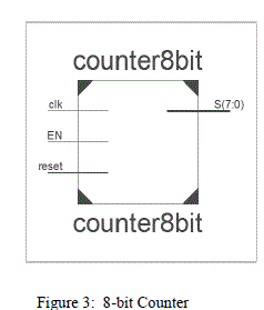 |
| Figure 3 shows the diagram of 8-bit counter. For each clock pulse counter is incremented by one. 8-Bit counter provides 8-Bit addresses to cache tag memory during writing and reading operation. C. cache tag comparator The 22-bit cache tag comparator Cache tag comparator is used to compare address requested by microprocessor and address stored in tag memory. 22-bit cache tag comparator is modelled using behavioural style of modelling in VHDL. |
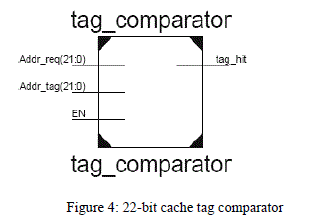 |
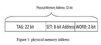
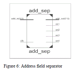
| Figure 4 shows the diagram of 22-bit cache tag comparator. To design 4-way set associative cache memory of 1KB, we need 4 set of such 22-bit Cache tag comparator. 22-bit Cache tag comparator compares 22-bit address requested by microprocessor and 22-bit address stored in tag memory. D.address field separator Address requested by microprocessor is 32-bit out of which 22-bit address is used to compare with tag address.8-bit address is used as a set address and 2-bit address is used as a offset word address. .figure 5 shows the physical memory address. |
 |
| To separate the addresses requested by microprocessor we designed address field separator as shown in figure 6. For example address requested by microprocessor is 32 bit out of which 22-bit address is used to compare with tag address.8-bit address is used to provide addresses to memory location and 2-bit address is used as a offset word. |
 |
E. Cache data memory |
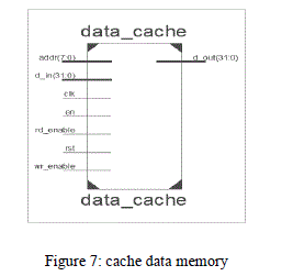 |
| Cache data memory is used to store the data from main memory as shown in the figure 7. We designed 4 ways of such 256 byte cache data memory to design 4 way set associative cache memory of 1KB.If address requested by microprocessor is present in cache tag memory then data related to hit address is given to microprocessor. |
V. CACHE CONTROLLER |
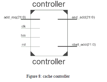
| Once the cache miss detect with the help of cache memory then cache controller will tracks the induced cache miss. To reduced cache miss we designed cache controller as shown in figure 8. Cache controller is designed on the basis of spatial locality of the reference. spatial locality of the reference means Given an access to a particular location in memory, there is a high probability that other accesses will be made to either that or neighboring locations within the lifetime of the program. if requested address is missing then cache controller generate the address range. This address range is nothing but the neighboring addresses of miss requested address. This address range given to the microprocessor by cache controller to replace addresses between this range into cache tag memory. This will reduce the cache misses |
 |
VI. RTL VIEW OF CACHE MEORY WITH CACHE CONTROLLER |
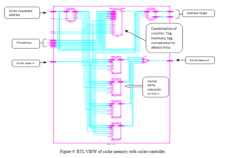 |
| The above figure shows the implementation of 4-way cache memory with cache controller. To achieve the synthesis of cache memory and cache controller, Xilinx ISE 13.1 platform is used. Initially addresses write into Cache tag memory through fill address when „weâÂÂ=1 and data is write into cache data memory through 32-bit data in. when 32-bit address requested by microprocessor then address field separator will separate address and used first 10 bit out of 32-bit for addressing purpose and 22-bit address is used for comparison with 22-bit addresses store in cache Tag memory. 22-bit cache Tag comparator is used for Comparison. If Requested address found in cache memory then cache hit will occurs and corresponding data related to requested address given to microprocessor through 32-bit data out. If cache miss will occurs then cache controller will generate address range related to requested address and this address range give to the microprocessor. To reduce the cache miss microprocessor will replace addresses within this range into cache tag memory. |
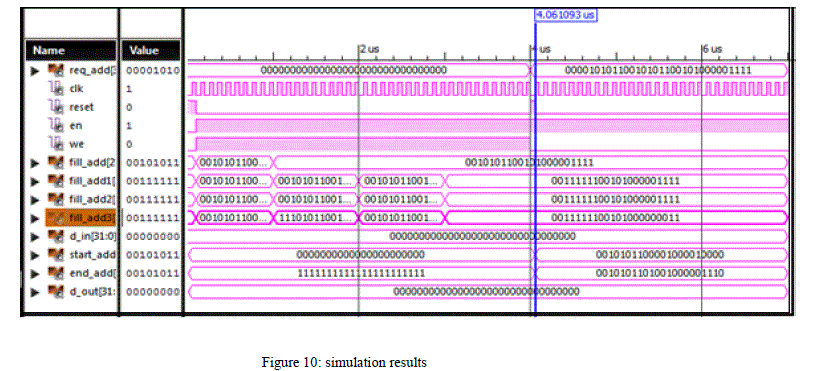
VII. SIMULATION RESULTS |
| Figure10 shows the simulation results of cache memory and cache controller for tracking induced cache misses. Cache memory with cache controller is designed using mixed style of modelling in a VHDL. In simulation results it is found that if address requested by microprocessor is matched with the address stored in cache tag memory then the cache hit will occurs, if not then cache miss will occurs. Once cache miss occurs cache controller generate the address range according to the requested missed address. |
 |
VIII. CONCLUSION |
| In this paper, we have presented design of cache memory on FPGA for detecting cache miss and design of cache controller for tracking induced cache miss in cache memory. Such an approach would be of great utility to many modern embedded applications, for which both high-performance and low-power are of great importance. This cache memory and cache controller may used in FPGA based processors. |
References |
|