International Journal of Innovative Research in Science, Engineering and Technology
ISSN ONLINE(2319-8753)PRINT(2347-6710)
ISSN ONLINE(2319-8753)PRINT(2347-6710)
Divyashree.M, Bhagya. P
|
| Related article at Pubmed, Scholar Google |
Visit for more related articles at International Journal of Innovative Research in Science, Engineering and Technology
In this paper basic CAM (Content Addressable memory) cell performs match and mismatch operation. CAM provides fast data search operation and it is also used as search engines. The CAM cell comprises of NAND cell block of array (1x8) and NOR cell block of array (4x32). Here in this paper 45nm technology (transistor sizing) with the supply voltage of 1V is used. The data stored in the CAM cell will be compared with the low swing search data on the search lines. The NAND and NOR match-lines of the cell blocks will reduce the power consumption of match lines. The proposed LSSL (Low Swing Search Line)-CAM architecture uses both NAND and NOR array in order to reduce the power and increase the speed. It also reduces the SL power by reducing the switching activity of search lines.
Keywords |
| LSSL-CAM, SL’s (search-lines), ML’s (match-lines), Switching activity, content addressable memory, low power. |
INTRODUCTION |
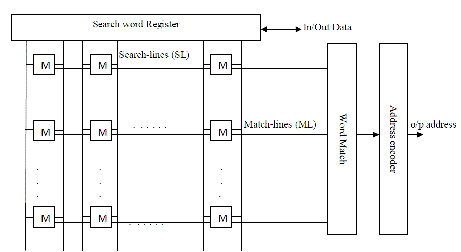
| In this paper, CAM (Content Addressable memory) compares the search data along with the stored data in a single clock cycle and returns the address at which matching data is found. CAM’s are used in databases, lookup tables, data compression, routers. CAM’s consume more power due to the presence of SL’s and ML’s and in search operation large amount of circuitry is active and consumes more power. Memory Cell consists of a word match circuit, search word register, and address encoder. The major power in CAM is consumed by highly capacitive ML’s and SL’s which are charged and discharged in every cycle. NAND CAM consumes least power but slow because only a highly-precharged ML is discharged through many transistors in series. NOR CAM is fastest but dissipates largest power because all highprecharged ML’s except one are discharged through many transistors in parallel. To achieve both low power and high speed both NAND and NOR CAM are combined together in LSSL (Low Swing Search Line)-CAM architecture. |
| The concept of LSSL-CAM (Low Swing search line) is been evolved from Byung-Do Yang and Lee-Sup Kim [2]. This gives knowledge about low swing switching voltage using NAND and NOR CAM’s together to get low power and high speed. Scheme proposed by K. Pagiamtzis [1] tells that the CAM compares the input search data with stored data and returns back the address where match is found. So here with emphasis of high capacity CAM, it gives the precharge-high scheme for sensing match-line as well as techniques that saves match-line power including lowswing sensing and current saving scheme. The technique introduced by H. Miyatake etal [4] tells that a new Cam cell with a pmos match-line driver reduces search rush current and power consumption, allowing a NOR-type match-line structure suitable for high speed search operation. This scheme by I. Arsovski and A. Sheikholeslami [4] gives an idea that a match-line sensing scheme that allocates less power to match decisions involving a large number of mismatched bits. In [5] Cache-CAM the main purpose of cache is to increase performance and main purpose of Cache-CAM is to reduce power consumption. |
 |
| Figure 3. gives an idea of CAM architecture which consists of array of memory cells, a search word register a word match circuit and address encoder. The above CAM cell can be implemented using either NAND CAM cells or NOR CAM cells. The memory cells are made of either binary CAM memory cells which can store “0” or”1”. The ternary CAM memory cells which can store “0”, “1” or “x” (don’t care). The CAM compares the search data with all arrays of memory cells and finds the matching word. The major amount of power in CAM cells is consumed by SL’s and ML’s. Many techniques have been invented to reduce the power consumption of ML’s. Many of them are based on high speed NOR type of CAM’s. Some techniques reduces the ML power by allocating less power to mismatched ML’s or by lowering the swing voltage of ML’s by using charge sharing ML scheme Reducing the number of activated ML’s by using pre-computation based CAM and also some techniques reduces the static power consumption of match-lines by allocating less power to mismatched ML’s. Some are based on low-power NAND-type CAM where the tree AND type ML scheme improves the searching speed. The Techniques are also been invented to reduce the SL power consumption. The pipelined Hierarchical search scheme reduces the search-line power by activating a few Sub-SL’s selected in the preceding pipeline stage but has an increased latency and area overhead due to pipelined stages. In this paper, a low power CAM using low swing search lines (LSSL-CAM) is being proposed. This method helps in reducing the SL power by comparing the stored data with low swing search data on SL’s. It also reduces the ML power by modifying the pulsed NAND-NOR CAM (PNN-CAM) architecture in [8]. |
ARCHITECTURE |
| A. Concept of Low Swing Search Line CAM |
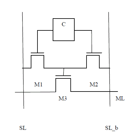
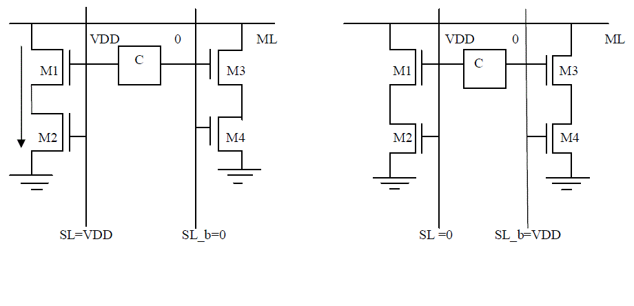
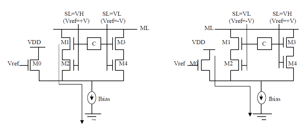
| Figure 4. Shows the operation of NOR-cell in a conventional NOR-CAM when the search data on a SL pair (SL and SL_b) is either matched or mismatched with the data stored. Initially the search lines are discharged to ground and ML is pre-charged to VDD. Then either the SL or SL_b is charged to VDD. In a match case the ML is discharged to ground and in a mismatch case the ML remains at VDD. |
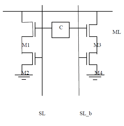 |
| Figure 5. Shows the operation of a NOR-cell in a proposed LSSL-CAM. To compare the search data along with the stored data on a SL pair, an NMOS transistor and bias current Ibias is added as shown. M0, M2 and Ibias acts like a differential amplifier. The matchline is discharged to ground or it remains at VDD depending on the voltages of SL and SL_b. In a mismatch case, the voltages of SL and SL_b are VH and VL. If the gate voltage of M2 is higher than M0 then the current Ibias flows through M2 as shown in Figure 5(a). The ML is therefore discharged to ground. In a match case the voltages of SL and SL_b are VL and VH and Ibias flows through M0. The ML remains at VDD. The currents in M0 and M2 changed according to VSL. The swing voltage of SL in LSSL-CAM is much smaller than in conventional CAM’s. |
 |
| B. NOR-cell Block in LSSL-CAM |
| In the operation of NOR-cell block in LSSL-CAM. The current supplying circuit generates an Ibias current for the circuit. In this schematic the Ibias is controlled by ML_EN and ML_ON in order to reduce power consumption of ML. Initially when ML_EN signal is “1” then ML is pulled to VDD. In match case ML is high so the signal ML_sense is zero which is an input to an inverter and further it is inverted to one and given as an input to an AND gate. The other signal to an AND gate is ML_EN which is “1” so the output at ML_NOR will be “1”. In mismatch case ML will remain at VDD and the ML_sense output will be one and the input to an AND gate is zero and one so the output at ML_NOR will be “0”.The ML sensing circuit helps in Identifying the voltage drop in ML. when the match line voltage “VML” becomes larger than the threshold voltage of PMOS transistor the ML_sense node is charged to VDD and ML_ON signal becomes zero. A small amount of current Ikeeper is used to decrease the voltage of ML. Ibias control scheme reduces the power consumption in all mismatched ML’s by limiting the voltage of VML. |
 |
| C. Architecture of LSSL-CAM |
| The LSSL-CAM architecture is based on pulsed NAND-NOR CAM (PNN-CAM) [8]. This architecture uses the advantages of both NAND-CAM and NOR-CAM. Where the NAND-CAM consumes a very small amount of power but it is slow in operation. Conversely in NOR-CAM it is very fast but consumes more amount of power. The proposed NAND-NOR architecture used in LSSL-CAM reduces the number of activated NOR-cell blocks. All NAND-cell blocks are activated but it consumes less power. The LSSL-CAM consumes small amount of power in ML’s by limiting the swing voltage VML. It uses a full swing voltage for few SL’s of NAND-cells and a low swing voltage on most of SL’s of NOR-cells. So the SL power will be significantly reduced. In the main architecture of LSSL-CAM it is divided into replica ML_block and L ML_block. Each match line block consists of an NAND-cell block and 4 NOR-cell blocks. The NAND-cell block and NOR-cell block have” K” NANDcells and “N” NOR-cells respectively. So in each ML_block there are totally “k+4xN” CAM cells. To generate the control signals needed for ML sensing operation, the LSSL-Cam uses replica NOR-cell block as in PNN-CAM [8]. The delays of GML_EN signal and ML_OE are well matched to send an exact signal to all ML_block. |
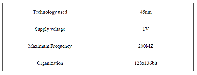
| Figure 7. Shows the schematic of implemented LSSL-CAM with an array of 128x136 bit CAM memory cells. The LSSL_CAM was implemented using 45nm technology with a supply voltage of 1V. The ML_block has an 8 bit NAND-cell block and 32 bit NOR-cell blocks. The 8 SL’s of NAND-cells uses full swing voltage and SL’s of NORcell uses a low swing voltage. In this LSSL-CAM initially when GML_EN signal is “1” if there is a match in NANDcell block then it is discharged to zero, then ML_en_b signal will be zero conversely ML_EN will be one. ML_EN signal activates the NOR-cell block and all high inputs are Anded together through a 4 input AND gate to get ML_output signal “1”. The output ML_NOR in replica ML_block is given as an input for SR Latch ” S” and input for “R” is from GML_EN so the output of SR Latch “Q” is zero when both input signals are high. For this output signal of SR Latch a delay is added by using 4 inverters in series and it is given as a 4th input of an AND gate and the ML_output is Zero. |
| D. Features of LSSL-CAM Architecture |
 |
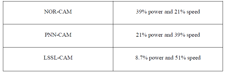
| E. Performance comparison |
 |
 |
CONCLUSION |
| In this paper, LSSL-CAM low swing search line technique is being shown. The CAM cells acts as an amplifier and also they compare the search data with the stored data in memory. The LSSL-CAM reduces the power consumption in CAM by using NAND type CAM and increases the speed by using NOR type CAM. It also reduces the power consumption of the match-lines by using the low swing NAND-NOR type match-lines. The CAM array is being designed and fabricated using 45nm technology with an supply voltage of 1V.The low swing search line CAM technique consumes only around 9% of power used by Conventional dynamic NOR-type CAM. Its maximum operating frequency is 200MZ. |