International Journal of Innovative Research in Science, Engineering and Technology
ISSN ONLINE(2319-8753)PRINT(2347-6710)
ISSN ONLINE(2319-8753)PRINT(2347-6710)
M.Saranya1, S.Mahalakshmi2, P.Saranya Devi3
|
| Related article at Pubmed, Scholar Google |
Visit for more related articles at International Journal of Innovative Research in Science, Engineering and Technology
The proposed method is based on minimum-cost maximum-flow formulation to globally determine the tree topology, which maintains load balance and considers the wirelength between pulse generators and pulsed latches. Experimental results indicate that the proposed migration approach can improve the power consumption by 12% and 13% with 7% and 70% skew improvements on average compared with the most recent paper on the industrial circuits and ISPD-2010 benchmarks, respectively. Minimizing the size of a clock tree is known as an effective approach to reduce power dissipation in modern circuit designs. However, most existing power-aware clock-tree minimization algorithms optimize power on the basis of flip-flops alone, which may result in limited power savings. To achieve a power and timing tradeoff, this paper investigates the pulsed-latch utilization in a clock tree for further power savings. This is the first paper to propose a migration approach to efficiently construct a clock tree with both pulsed-latches and flip-flops.
Keywords |
| Clock tree migration, dynamic power reduction, pulse generator, pulsed latch. |
INTRODUCTION |
| In current circuit designs, the most common storage element is a D-type flip-flop that consists of two latches (master and slave) triggered by a clock signal. This type of design makes it easier to apply static timing analysis (STA) for timing verification. As transistor counts of a flip-flop are two times than that of a single latch, latches are superior to flip-flops in terms of area, transition time, and power dissipation. However, it is difficult to perform STA on latch-based circuits because of data transparency. A pulsed-latch-based design style was adopted for dynamic power. Pulsed latches are latches triggered by a brief clock signal generated from a pulse generator. When the pulse clock waveform triggers a latch, the latch is synchronized with the clock and its timing behaviour is similar to an edge-triggered flip-flop. Hence, STA can be applied to the pulsed-latch clock tree. Power consumption has become a crucial issue in highperformance circuits because the number of transistors has increased substantially. Several techniques are proposed to reduce total power of a chip, such as multiple supply voltages clock gating and clock-tree minimization. Because of heavy pipeline designs and high-frequency signal switching, a clock tree is known to be a major contributor to power dissipation. The clock tree accounts for a significant portion of total power consumption and consumes 20%–40% of total power in synchronous circuit. Therefore, the chip power can be greatly reduced by decreasing the clock-tree power. The power dissipation of a clock tree can be reduced by decreasing total (clock) wire capacitance. Therefore, pulsed-latch designs have both advantages of latches and flip-flops: they offer easier timing verification and less power consumption As in an 20% reduction in total dynamic power consumption can be achieved in practice.Although pulsed latches can effectively reduce power consumption, most current design flows are built for flip-flop designs. To adopt pulsed latches for a current design flow, designers might change the circuit description in high-level synthesis. However, this modification incurs excessive costs and causes high complexity in physical-synthesis stages. Therefore, in this paper, we present an efficient pulsed-latch migration approach in physical design to minimize the cost of utilizing pulsed latches under the current design flow. In pulsed-latch designs, a pulse generator is indispensable |
PRELIMINARIES |
| Most design flows are based on a flip-flop-based circuit However, if designers attempt to resynthesize pulsed latches and perform corresponding processes such as placement and routing, it inevitably introduces excessive extra costs. Therefore, in this paper, we propose an efficient yet effective migration approach to reduce the effort of transforming a flip-flop-based clock tree into a pulsed-latch-based.Given a flip-flop-based clock Comparisons of pulsed-latch migration flows. (a) Migration flow proposed in proposed migration flow with mixed structure.we apply migration methods to obtain a new clock tree with a mixture of pulsed latches and flip-flops. shows a comparison between previous paper and the proposed design. A pulsed-latch migration with a single-type pulse generator. However, the migration method should contain a mixed structure of pulse latches and flip-flops. Moreover, the driven load of pulse generators may be different, and replacing generators with smaller generators will further reduces power consumption |
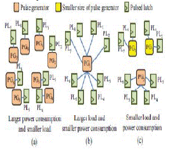 |
| Dynamic power is mainly derived from circuit operation. The power dissipation of a clock tree often dominates the total power consumption in a circuit. Therefore, this paper focuses on dynamic power, which can be computed. This type of design makes it easier to apply static timing analysis (STA) for timing verification. . To achieve these goals, this paper presents a new clock tree with a mixed structure of pulse latches and flip-flops that is capable of multitype pulse-generator insertion.There are two major components of power dissipation in a circuit: static power and dynamic power. Static power, which is the result of the leakage current of transistors, consumes power even when the circuit is not operating. As transistor counts of a flip-flop are two times than that of a single latch, latches are superior to flip-flops in terms of area, transition time, and power dissipation. However, it is difficult to perform STA on latch-based circuits because of data transparency. A pulsed-latchbased design style was adopted for dynamic power reduction .Pulsed latches are latches triggered by a brief clock signal generated from a pulse generator. When the pulse clock waveform triggers a latch, the latch is synchronized with the clock and its timing behavior is similar to an edge triggered flip-flop. Hence, STA can be applied to the pulsed-latch clock tree. Therefore, pulsedlatch designs have both advantages of latches and flipflops: they offer easier timing verification and less power consumption . As in , an 20% reduction in total dynamic power consumption can be achieved in practice. Although pulsed latches can effectively reduce power consumption, most current design flows are built for flip-flop designs. pulsed-latch circuits, the largest-size pulse generators are inserted to drive pulsed latches.To adopt pulsed latches for a current design flow, designers might change the circuit description in high-level synthesis. However, this modification incurs excessive costs and causes high complexity in physical-synthesis stages. Therefore, in this paper, we present an efficient pulsed-latch migration approach in physical design to minimize the cost of utilizing pulsed latches under the current design flow. In pulsed-latch designs, a pulse generator is indispensable to generate a clock pulse, but consumes more power than a pulsed latch and a buffer. Although pulsed latches can reduce power dissipation, the total power of the clock tree may increase because of additional pulse generators. Thus, there is a tradeoff between the pulse-generator insertion and pulsed-latch substitution. As the clock pulse is sensitive to output load, it is essential to control the load of a pulse generator for potential pulse degradation . Additionally, if designers do not limit the number of pulse latches driven by a pulse generator, the number of fanoutsIn the pulse generator may be too large, which could lead to routing congestion. Therefore, two major factors must be considered to control the output load: 1) the pulsegenerator driving load cannot exceed the maximum tolerable load defined in the library and 2) the number of pulsed latches driven by a pulse generator should be smaller than the maximum fan out number. As pulse generators consume large amounts of power in pulsedlatch circuits, it is critical to reduce the pulse-generator power. Proposed multi type pulse generator insertion to reduce the unnecessary power dissipation. Considering clock gating of Then, to further reduce power consumption, this method replaces the largest-size pulse generators with smaller-size ones if there are no constraint violations. As a result, the power consumption can be further reduced. However, existing methods of clock-tree minimization are primarily based on flip-flops and focus on wire length minimization alone, which may limit achievable power savings. In current circuit designs, the most common storage element is a D-type flip-flop that consists of two latches (master and slave) triggered by a clock signal. This type of design makes it easier to apply static timing analysis (STA) for timing verification. As transistor counts of a flip-flop are two times than that of a single latch, latches are superior to flip-flops in terms of area, transition time, and power dissipation. |
 |
| High power dissipation of an SoC will not only increase its system costs but also affect the product life time and reliability. To optimize the power consumption, many low-power design techniques have been introduced, such as clock gating replacing non-timingcritical cells with their high-Vtcounter parts, power gating , creating multi-supply-voltage designs dynamic voltage/ frequency scaling and minimizing clock network. To reduce runtime, the proposed approach uses a Voronoi diagram to divide the design into several polygons for providing locality information among pulsed latches. We solve the problem with a minimumcost maximum-flow method to globally determine the clock-tree topology, which maintains the appropriate load balance while considering the wire length between pulse generators and pulsed latches. |
ALGORITHM |
| Among these techniques, minimizing clock network is very important in reducing power consumption of an SoC because it accounts for up to 50% of dynamic power of the chip and the dynamic power is the dominant power source, which accounts for 75% of total power consumption of an SoC .Resent studies have proposed various approaches to minimize clock network, including buffer sizing placement optimization of registers , and applying multi-bit flip flops(MBFFs) , or multi-bit registers, or register banks.The problem of power optimization with MBFFs at the post-placement stage. It present a new problem formulation for the application of multi-bit flip flops, which simultaneously minimize total flip-flop power consumption and interconnecting wire length such that both placement density and timing slack constraints are satisfied. Based on the problem formulation, we propose a novel post placement power optimization flow together with the flip-flop grouping and MBFF placement algorithms to solve the addressed problem. process. We conducted the experiments on five industrial circuits and eight circuits from ISPD-2010 clock network contest [23]. As we did not consider the obstacles in this paper, we only used the sink locations while ignoring the obstacles. |
 |
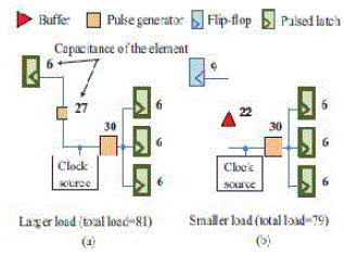
| Ideally, pulsed latches become edge-triggered devices for a pulse of zero width. However, in practice the pulse width has to be large enough for captureflip flop are memory elements that are commonly used in the design of sequential circuits such as finite-state machine controllers and pipelined circuits.It formulate the flipflop grouping problem as the m-clique finding and maximum-independent-set sub problems. Finally, we introduce the progressive window-based optimization technique to reduce placement deviation and improve runtime efficiency of our algorithms. Experimental results show that our approach is very effective in reducing not only flip-flop power consumption but also clock tree and signal net wire length when applying multi-bit flip-flops to a design at the post-placement stage.Pulsed latches are latches driven by a brief clock pulse. They retain the design advantage of latches while offering flip-flop like timing verification and optimization, since they behave like flip-flops due to a short period of transparency. Several types of pulsed latches have been proposed, mostly for high performance microprocessor designs. For instance ,pulsed latches are used for timing-critical paths while flip-flops are used for the paths that are not critical to timing . The application of pulsed latches to ASICs has been reported recently; the substitution of pulsed latches for some flip flops can yield a 20% reduction in total dynamic power consumption. Experimental results indicate that the migrated clock tree can reduce power consumption by 12% and 15% and achieve a 7% and 70% skew improvements on average compared with the most recent paper on the industrial circuits and ISPD-2010 benchmarks.The first experiment compared flip-flopbased circuits, pulsed-latch-based circuits, and the proposed pulsed-latch migration scheme (with mixed sink types and multitype pulse generator) on industrial circuits. Table IV lists the comparisons of power dissipation improvement for different types of sinks. The columns Sinks, Bufs, PGs, and Wires list the power consumption of sinks, buffers, pulse generators, and wires, respectively. The total power, column Total, is the summation over the power dissipation of sinks, wires, and drivers. Columns #FF and #PL list the number of flip-flops and pulsed latches for mixture sink types, respectively.To prevent pulse distortion, the total load of a pulse generator cannot exceed the defined tolerable load and the maximum fanout constraint during the migration |
PROBLEM FORMULATION |
| Pulsed latch-based circuits using a single pulse width, which is the conventional approach, cannot take advantage of time borrowing due to their short period of transparency. This can be alleviated by employing sequential optimization techniques such as retiming or clock skew scheduling . However, the use of retiming often causes a large increase in the number of latches thus limiting its practical use; and it can also have an impact on the verification methodology. Conventional clock skew scheduling assigns an arbitrary amount of skew to each latch to balance the delay between the combinational blocks. It has been shown that the maximum difference in clock arrival times that can be practically realized are less than 10% of the clock period in 0.18-μm technology , or 10% to 16% in 0.18-μm and 0.13-μm technologies . This is also true in a clock grid where only a very small amount of skew can be realized. This paper presents a method of reducing the power consumption of the clock tree by modifying the tree topology and minimizing the clock skew. In addition to minimizing the dynamic power of a clock tree, it is also necessary to control the amount of pulse generators as introduced in Section I. Since the tree topology changes after pulse-generator insertion, the clock skew might increase. As a result, it is important to consider the skew issue during the clock-tree reconstruction. For the transition time of each cell, we applied STA to derive the timing information. When calculating the timing information, we also check each cell to verify whether the input net transition time or total net capacitance exceeds the maximum value defined in the library. In summary, the problem can be formulated as follows.we consider the generators with the largest driving capabilities the main difference between the algorithm proposed in and to obtain better results, we cluster all pulsed latches rather than local reclustering..Algorithm 1 shows the pseudocode for the proposed clustering procedure. Initially, regard each sink as an individual group, and calculate the Manhattan distance between each pair of sinks in the pulsed-latch set PL. Sort the distance set in the ascending order, and preferentially select the shorter distance such that the minimum distance between two sinks is a closer pair. If two sinks are located in different groups, they can be merged into the group with the shortest distance if all the constraints are satisfied is the grouped total load capacitance of giand g j . To reduce power consumption, we merge pulsed latches by considering the tradeoff between the number of pulse generators and wirelength (line 8). This is a tradeoff method to achieve better power reduction than an approach focused on minimizing the number of pulse generators alone. |
EXPERIMENTAL RESULTS |
| The algorithm is implemented in the C/C++ language and the experiments are performed on a Linux machine with 2-GHz Intel Xeon CPU with 16-GB memory. The proposed STA method is developed by using the source code from Lin et al. To calculate the transition time for each cell, STA is used to derive the timing information with the synopsys. cell library. To show the comparison between the pulsed-latch-based circuit and the migrated clock tree with mixed sinks, the pulsed-latch-based clock tree. |
 |
| When calculating the timing information, it isalso necessary to assess each cell to determine whether the input net transition time or total net capacitance exceeds the maximum value defined in the library. The levelled clock tree synthesis and the levelled buffer insertion are performed to construct the initial buffered clock tree.The wire load is calculated as the multiplication of total wire length between a pseudo pulse generator and the pulsed latches and wire load constant presented in [20]. Additionally, we estimate the connection wire length by calculating the Manhattan distance.We used the algorithms to construct the initial buffered clock tree with zero skew. At each clustering iteration, a pseudo pulse generator is placed at the centre position of a group to determine whether the constraints can be satisfied. Considering Cmax, the total load capacitance of a group is the sum of the total sink load in the two selected groups and the connection wire load between each sink and the pseudo pulse generator. |
 |
| To provide a reasonable setting, we set the maximum tolerable load and maximum fan-out constraint of the multitype pulse generator.To prevent pulse distortion, the total load of a pulse generator cannot exceed the defined tolerable load and the maximum fan-out constraint during the migration process. To optimize the power consumption, many low-power design techniques have been introduced, such as clock gating replacing non-timing-critical cells with their high-VT counter parts, power gating , creating multi-supply-voltage designs dynamic voltage/ frequency scaling and minimizing clock network. The approach in sets the maximum tolerable load of a pulse generator as the maximum output load of a small-size buffer. However, the maximum tolerable load of pulse generator should be much smaller than that to avoid pulse degradation. We conducted the experiments on five industrial circuits and eight circuits from ISPD-2010 clock network contest. As we did not consider the obstacles in this paper, we only used the sink locations while ignoring the obstacles. The statistics of the industrial circuits and ISPD-2010 benchmarks are listed in where column Test cases lists the circuit name, and columns Chip size and #Flip-flops list the chip size and number of flip-flops, respectively. Clustering can be considered the most important unsupervised learning problem; so, as every other problem of this kind, it deals with finding a structure in a collection of unlabelled data. A loose definition of clustering could be “the process of organizing objects into group’s members are similar in some way.A cluster is therefore a collection of objects which are“similar” between them and This method of reducing the power consumption of the clock tree by modifying the tree topology and minimizing the clock skew. In addition to minimizing the dynamic power of a clock tree, it is also necessary to control the amount of pulse generators as introduced in. Since the tree topology changes after pulse-generator insertion, the clock skew might increase. As a result, it is important to consider the skew issue during the clocktreereconstruction. For the transition time of each cell, we applied STA to derive the timing information. When calculating the timing information, we also check each cell to verify whether the input net transition time or total net capacitance exceeds the maximum value defined in the library. This section demonstrates the performance of multi type pulse-generator insertion.The first experiment compared flip-flop-based circuits,pulsed-latch-based circuits, and the proposed pulsed-latch migration scheme (with mixed sink types and multitype pulse generator) on industrial circuits. The lists are comparisons of power dissipation improvement for different types of sinks.The cell library of multitype pulse generators we used are based on. It shows the cell library of multi type pulse generators. Row Cap and Load list the cell capacitance and maximum tolerable load of pulse generators, respectively.In small cases, the algorithm without a Voronoi diagram can still adequately manage the problem. |
 |
| However, the runtime increases significantly as the number of sinks increases because of the high complexity of network-flow modeling. Experimental results show that when the Voronoi diagram is applied, the worst skew improves by 93% and 29% and the power consumption is also reduced compared with algorithms without a Voronoi diagram on industrial circuits and ISPD-2010 benchmarks, respectively. These improvements confirm that the proposed Voronoi diagram construction not only decreases the runtime, but also maintains the solution quality. |
CONCLUSION |
| In this paper, we proposed an efficient clock-tree migration approach that can migrate a flip-flop-based clock tree into a pulsed-latch-based one for dynamic power reduction. To prevent pulse degradation, the tolerable load of a pulse generator and the number of pulsed latches driven by a pulse generator were considered during pulse-generator insertion. To further reduce the power dissipation of pulse generators, we enabled multitype pulse generators and identified the pulse generators with suitable size to drive pulsed latches. Considering the tradeoff between the additional power of multitype pulse-generator insertion and the power savings of pulsed-latch substitution, not all flip-flops were replaced. This allows the migrated clock tree to be constructed with a mixed structure of latches and flipflops. To determine the topology configuration and simultaneously minimize the wirelength and load balance, we applied a minimum-cost maximum-flow formulation to solve the pulsed-latch-clustering problem. Experimental results indicated that the proposed migration approach can improve both power consumption and skew compared with the most recent research on the industrial circuits and ISPD-2010 benchmarks, respectively. An efficient clock-tree migration that can migrate a flip-flop-based clock tree into a pulsed-latch-based one for dynamic power reduction. To prevent pulse degradation, the tolerable load of a pulse generator and the number of pulsed latches driven by a pulse generator were considered during pulse-generator insertion. To further reduce the power dissipation of pulse generators, To enabled multi type pulse generators and identified the pulse generators with suitable size to drive pulsed latches. Considering the trade off between the additional power of multi type pulse-generator insertion and the power savings of pulsed-latch substitution, not all flip-flops were replaced. This allows the migrated clock tree to be constructed with a mixed structure of latches and flip-flops. To determine the topology configuration and simultaneously minimize the wire length maintain load balance, we applied a minimum-cost maximum-flow formulation to solve the pulsed-latch-clustering problem. Experimental results indicated that the proposed migration approach can improve both power consumption and skew compared with the most recent research on the industrial circuits and ISPD-2010 benchmarks, respectively. To achieve 40.25% power reduction than existing system.In the future work, to apply a DVFS(Dynamic voltage and frequency scaling) algorithm. It is one of the most effective method for low power consumption. |
References |
|