Keywords
|
| SoC (System on Chip), CAD (Computer Aided Design), VGA (Video Graphics Array), Quartus II, Qsys. |
INTRODUCTION
|
| All Embedded Systems which is the combination of both hardware and software components working together to perform a specific application. Nowadays, the design of embedded systems is become difficult due to the constraints on accessing area, usage of memory size, power consumption and performance of the system [1]. Added with designers facing time to market deadlines. Altera's Nios II processor is the world's most versatile processor [18]. It is more suitable for wide range of embedded computing applications. The embedded processor cores are integrated into most System on Chip (SoC). The processor cores can be designed to be dedicated for a SoC and reusing of generic processors is often preferred due to time to market constraints. The processor core which is adaptable to many different things. It can be completely applied using logic synthesis [5]. The Nios II processor which is provided by Altera family to be implemented in FPGA and also lots of softcore processors available in the market. Nowadays, growing complexity of applications has made design of challenging. The most effective way to implement area and power consumption for efficient architectures is to design fully dedicated ones. It provides options for configure the softcore processor. The several softcore processors are Nios II, Microblaze, Picoblaze, Xtensa are the softcore processors provided by Altera, Xilinx, Tensilica respectively. There are several use of softcore processors available for the developer of an embedded system. The softcore processors which is flexible, hence it can be customized for for a specific application need [2]. Field Programmable Gate Array (FPGA) is configured by the end user. In FPGA, We can test and validate our design. Instead of ASIC, it is useful for low production, simple design cycle and time to market. |
| The Organisation of the paper is as follows: Section II provides Design cycles for FPGA and ASIC In Section III gives the Implementation of Hardware & Software Codesign. We conclude in Section IV and with some comments on future work. |
DESIGN CYCLES FOR FPGA AND ASIC
|
| Due to the efficient design cycle of FPGAs, it is considered for developing rapid prototypes during the embedded system design process. With the use of prototypes, it is also important that simulations be performed to further speed up the design process. Simulations are useful even before developing a prototype of the device or system. It is preferable that both are used when developing. FPGA should be used instead of ASICs. FPGA have simple design cycle compared to ASIC. It is faster time to market. The functionality of the FPGA can be customized in the field. |
| 1. Hardware And Software Codesign |
| The Hardware and software codesign of today’s systems to trade-off performance, power and dependability in multicore processors. In Software based techniques are severely limited by observability and control ability of the hardware due to strict abstraction layers. This gives rise to the problem of matching the performance requirements of a specific application of a processor. |
| The application design consists of three types of development: hardware design and software design and System Design. |
| Hardware Design |
| The hardware design which is done by Qsys Builder available in the Quartus II. Using Qsys Builder we can specify the Nios II processor cores, memory, and required other components. It interconnect the logic automatically to integrate the components in the hardware system. The Qsys Builder which is nothing but system integration tool [14]. It saves significant time & effort in the FPGA design process by automatically generating interconnect logic to connect IP functions and subsystems |
| Qsys Builder |
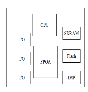
| The Qsys builder which is used to integrates the components in the hardware system. The Qsys which allows the users to put together a system using already available and or custom components. After interconnecting components get downloaded into the target board. Below Fig. 3. Represents the general system which contains processor and several I/O components in the design then the system is bulky and costly. |
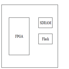
| In Fig.4. It represents the small system of hardware components. The system gets reduced by using Qsys builder. This small system will give optimized performance. The errors also get reduced and debugged easily because of this small system. |
| Software Design |
| The Nios II Integrated Development Environment (IDE) is the main softwaretool provided by Altera when designing using Altera FPGAs. This software tool is mainly used when the FPGA has the capability of housing a softcore, Nios, embedded processor. The Nios II IDE contains the following main functions for software development |
| • Project Manager |
| • Editor and Compiler |
| • Debugger |
| • C-to-Hardware (C2H) Acceleration Compiler |
| • Flash Programmer |
| • Nios II Software Build Tools |
| The Nios II IDE is based on the open, extensible Eclipse IDE project and the Eclipse C/C++ Development Tools Project [16]. The project manager automates setup of the C/C++ application project and system library projects. Nios II IDE provides software code examples (in the form of project templates) to bring up working systems as quickly as possible. Each template is a collection of software files and project settings. Custom source code can be added to the project by placing the code in the project directory or importing the files into the project. Full-featured source editor and C/C++ compiler is within the Nios II software. |
| System Design |
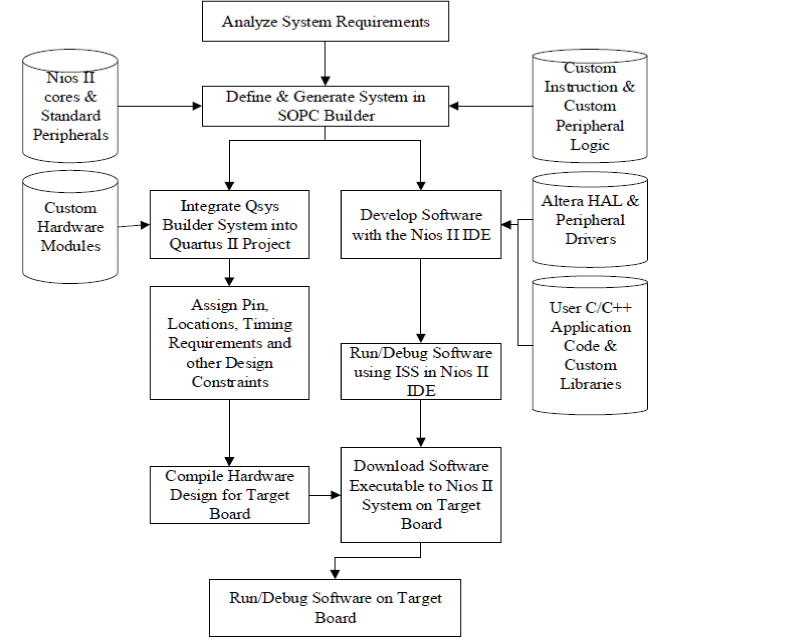
| The System Design is the integrating of both hardware and software. The CAD design tools such as Quartus II, Qsys, and Nios II IDE used to develop the application with high performance. In this design we can assign memory for our application. In normally processors can’t able to change the size of memory. It is difficult for running the complex task. In SoC design it is easy to change the memory size and also reduce the memory access. In Fig. 5 It shows the hardware and software codesign. The hardware portion of the design process consists of using Verilog or VHDL to define custom hardware, using parts from the library, or gate level parts. Often a design environment or board contains intellectual property that can be integrated into the design. Configurable regions or parts are developed and available in design environments. These are used for commonly used components such as arithmetic functions. The use of embedded processors in the design is a major decision. The decision depends on the application and design parameters. |
| The software process choices depend on the tools available to the designer. Using a supported processor core assist when designing the software for the embedded system because of the software tools that come with the processor. When completing the software part, it can also be seen as a hardware block with inputs and outputs. The external connections to the software block either connect to an external port of the embedded system or there are interconnections between the hardware and software parts of the system. |
IMPLEMENTATION
|
| The Prototyping platform using FPGA Altera DE0 development board has the cyclone III FPGA chip.The CAD tools that are available for the Altera DE0 board are Altera Quartus, Qsys builder and Nios IDE. The Quartus is the foundation for FPGA logic design. The Qsys (system on integration) Builder is accessed through Quartus and it is to customize the Nios II soft processor core. Once the hardware has been specified, the C/C++ software application can be developed using Nios II IDE. The peripherals of the development board range from the JTAG programming interface to the VGA ports. The board consists of internal clock as 50 MHz oscillator are part of the development board. The Cyclone series of FPGAs all contain Nios II embedded processors, graphics hardware acceleration, memory interface and the Avalon switch fabric (ASF). The embedded processor available for the cyclone III FPGA is a softcore processor. Nios II processors implement a 32-bit instruction set based on a RISC architecture. It is a soft-core processor, the designer can choose from a countless of system configurations, choose the best CPU IP core as well as selecting peripherals. |
| The Design flow consists of two stages Hardware design and software design. |
| Hardware Design |
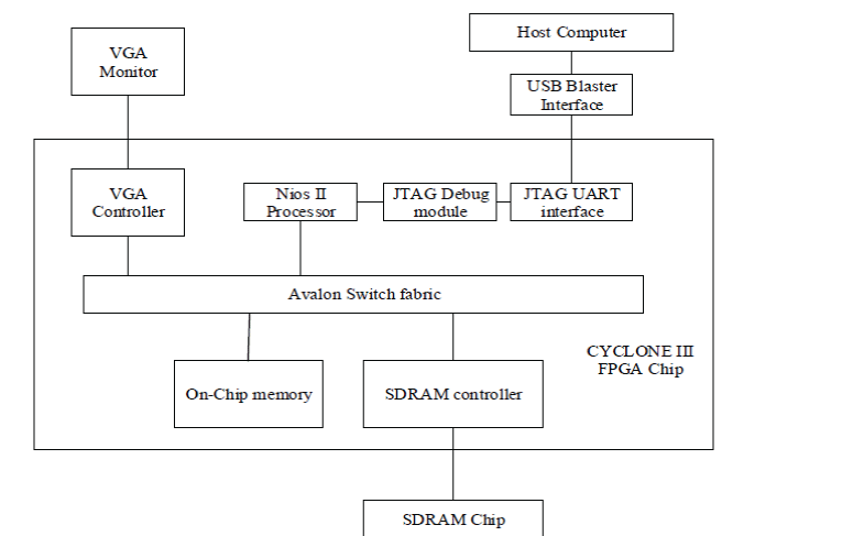
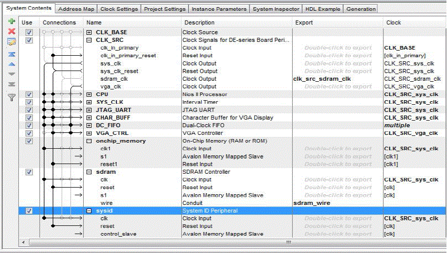
| The hardware design by using the Qsys Builder. The Qsys consists of IP core several components which is already available in the Qsys builder. The hardware is broken into three components namely Nios II system, SDRAM, VGA controller. The Fig. 8 which shows that SoC for hardware design. |
| Nios II processor |
| The Nios II processor is the world’s most versatile processor. There are three types of Nios II CPU cores available. The choice of the CPU core provides the designer with the opportunity to change the design to the application demands. In [15], the table below summarizes the types of cores and the features of each one. |
| Avalon Switch Interface |
| Nios II uses the Avalon switch fabric as the interface to its embedded peripherals. When compared to a traditional bus in a normal processor based system it only gives one bus master access the bus at a time. But in Avalon switch fabric, using a slave side arbitration so multiple masters operate simultaneously. |
| VGA Controller Core |
| The VGA core supports 640 x 480 resolution, it can support three display modes pixel mode, character mode, and character overlay mode. In a 640 by 480 pixel mode and 60 Hz refresh rate, there is approximately 40 ns per pixel. In our design first analysis with character buffer it is used to display the characters on VGA then after that with pixel buffer, the VGA core uses the RGB color model to the VGA display. In character mode it is used to display the characters. Two sizes are supported in the character buffer. They are 8x8 here the character occupies an 8x8 in VGA which means that 80 characters can be displayed per line and the VGA core can support up to 60 lines. At last 16x16 it occupies 16x16 in VGA, it means that 40 characters can be displayed per line and the VGA core can support up to 30 lines. The fig. 5 which shows the SoC design for character get displayed on the VGA monitor while the SoC design get successful in the Qsys integration tools. In Pixel mode, the VGA core uses the RGB color model, it have the following color space settings are available. It is 16-bit color mode that is Red and blue have 5-bit color spaces. Whereas green has a 6-bit color space. Then it have 8-bit color mode for grayscale [8]. |
| The major hardware circuit is designed based on the resources of DE0 development board. The Cyclone EP3C16F484 FPGA as the main chip [13]. The Qsys builder achieves the connections of various IP core then it is integrated with Quartus II, it completes the work of Nios II softcore processor and connected peripherals. The Nios II processor was set up using the Qsys builder. The processor components are selected and added as shown in Fig. 5. |
| Integration of SoC into Quartus II |
| The SoC design which is integrated into the HDL in Quartus II. The HDL means using VHDL, Verilog or schematic. But here Verilog was used to implement the SoC design. The programmer allows us to configure all Altera devices supported by the Quartus II software with files generated by the compiler. The Quartus II compiler generates programming files that the programmer can use to program or configure a device with Altera programming hardware. The USB Blaster is used to interface with DE0 board and PC. In JTAG programming mode is used to program the device. The hardware design get loaded to the FPGA device. It will not run the application. It get runs the application only after the software part for the application loads to the board then if it is successful design means it will run the application. |
| Software Design |
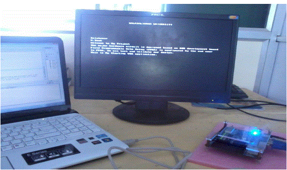
| The main function of the software is to initialize and control the peripherals. The software aspect is straightforward, but the uncertainty is present when using the HAL and direct register functions. he VGA controller that is available for the DE0 board contains a limited amount of function support. It is unclear as to how to control the VGA, but during implementation a better understanding can be gained. Once experience is gained in using the functions and libraries within the Nios II IDE, implementation of the application software will be get quickly completed.The software for the application is written in the Nios II IDE. It is written using C or C++. The Nios II library functions were used to implement the VGA controller core and SDRAM.The C code for application was written then performed compilation and debug. The successful compilation of the application generated the .elf file. The .elf file get downloaded to the DE0 Board through USB blaster cable. Then after that run the application it was successfully runs in our design. Fig. 6 shows the implementation of VGA monitor interfaced with FPGA board using CAD tools. It shows the result of our research and experiment. |
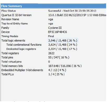
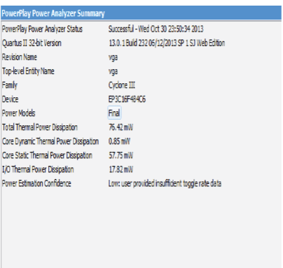
| In Fig 7 and Fig. 8 shows the analyses report of resources used and also thermal power dissipation of our design. |
CONCLUSION
|
| This paper demonstrated the hardware and software codesign of using Nios II processor was done. The design of an embedded system is implemented on FPGA with the help of HDL. While designing of an embedded system the memory and power of an application get optimized. It utilized only about 26% resources. The VGA core function to draw pixels across the screen was tested. In future, to design SoC for SD card using Qsys builder. The SD card contains the test image. With the help of Nios II Eclipse IDE software application read the test image from SD card that the image to be display on the VGA monitor. In meanwhile, the energy and power to be optimized for that design. |
ACKNOWLEDGEMENT
|
| This research project would not have been possible without the support of my guide, teachers and friends. The authors are grateful to the management and the head of the Institution of Kalasalingam University for giving all necessary support and providing facilities for making this research paper a successful one. This knowledgably guidance helped me to complete up to this stage and hope will continue in further research. |
Tables at a glance
|
 |
| Table 1 |
|
Figures at a glance
|
 |
 |
 |
 |
| Figure 1 |
Figure 2 |
Figure 3 |
Figure 4 |
|
 |
 |
 |
 |
| Figure 5 |
Figure 6 |
Figure 7 |
Figure 8 |
|
References
|
- Rabie Ben Atitallah , Eric Senn, Daniel Chillet, Mickael Lanoe and Dominique Blouin “An Efficient framework for Power- Aware Design of Heterogeneous MPSoC” IEEE Transc. On Industrial Informatics, Vol 9, No. 1, Feb 2013.
- Peter Yiannacouras, J.Gregory Steffan, and Jonathan Rose “Exploration and Customization of FPGA-Based Soft Processors” IEEE Transc. On Computer-Aided Design of Integrated ciruits and Systems, Vol. 26, No. 2, Feb. 2007.
- Bertrand Le Gal, Christophe Jego “Softcore Processor Optimization According to Real-Application Requirements” IEEE Embedded Systems Letters, Vol.5, No.1, March 2013.
- Mike Dyer, Amit Kumar Gupta and Natalie Galin “Nios II Processor-BasedHardware/Software Co-Design of the JPEG 2000 Standard” Nios II Embedded Processor Design contest-2005.
- Jason G.Tong, Ian D.L.Anderson and Mohammed A.S.Khalid “Soft-Core Processors for Embedded Systems” The 18th International Conference on Microelectronics (ICM) 2006.
- PONG P.CHU” Embedded SoPC design with Nios II processor and Verilog examples” A John Wiley & Sons, Inc., Publication 2012.
- “VGA CORE for Altera DE1/DE2 Boards” Altera Corporation University Programs, Oct 2006.
- Jerraya, A. “Long Term Trends for Embedded System Design” IEEE Euromicro symposium On Digital System Design, Sep 2004.
- Maxfield, C. “The Design Warrior’s Guide to FPGAs.” Elsevier. 2004.
- “Quartus II Version 7.2 Handbook Volume 5: Altera Embedded Peripherals.” Altera Corporation.
- Altera “DE0_User_Manual for DE0 series Board” Terasic, May 2009.
- “Embedded Software.” Altera Corporation.
- “DE0 Development and Education Board”, Altera Corporation. DE0 CD-ROM. DE0 Schematics PDF.
- “Quartus II Version 13 Handbook: Introduction to the Altera Qsys System Integration Tool.” Altera Corporation.
- “Nios II 7.1 Processor Reference Handbook. “Altera Corporation.
- “Nios II 7.1 Software Developer’s Handbook.” Altera Corporation.
- “Cyclone III Device Handbook.” Altera Corporation.
- Altera Corporation Website, www.altera.com.
- Maxfield, C. “The Design Warrior’s Guide to FPGAs.” Elsevier. 2004.
|