Keywords
|
| QCA, Full adder, Ring counter, T FlipFlop |
INTRODUCTION
|
| A.QCA cell |
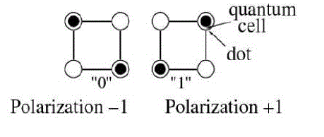
| A quantum-dot cellular automata (QCA) is a square nanostructure of electron wells confining free electrons. Each cell has four quantum dots which can hold a single electron per dot. The four dots are located at the corners of the cell and only two electrons are injected into a cell. By the clocking mechanism, the electrons can tunnel through to neigh boring cells during the clock transition by the interaction between electrons. A high potential barrier at the settled clock signal locks the state and results in a local polarization which is determined by Coulombic repulsion. The two electrons reside in opposite corners so that two polarizations are possible as seen in Fig. 1. Those two binary states can be used to make QCA cell[1] a storage cell, a computing cell, or a wire. |
| B. Signal flow |
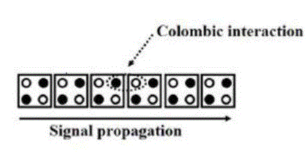
| A series of QCA cells act like a wire. An illustration of a QCA wire is shown in Fig. 2. During each clock cycle half of the wire is active for signal propagation, while the other half is stable. During the next clock cycle, half of the previous active clock zone is deactivated and the remaining active zone cells trigger the newly activated cells to be polarized. Thus signals propagate from one clock zone to the next. |
| C.QCA Clock |
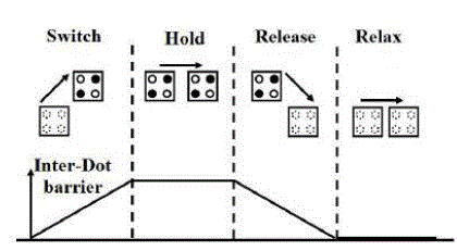
| The circuit area is divided into four sections and they are driven by four phase clock signals. As shown in Fig. 3, there is a 90 degree phase shift from one section to the next. In each clock zone, the clock signal has four states: high-to low, low, low-to-high, and high. The cell begins computing during the high-to-low state and holds the value during the low state. The cell is released when the clock is in the low-to-high state and inactive during the high state. |
| The QCA clocking [3] signal is used to control the signal propagation along the QCA cells arrangement. There are Four-Different Clocking Phases such as „SWITCH, HOLD, RELEASE and RELAX?. |
| SWITCH: |
| During this phase, the inter-dot barriers are slowly raised and the computation takes place according to QCA cell arrangement. |
| HOLD: |
| In this phase, the inter-dot barriers are kept high and the QCA cells retain their states. |
| RELEASE: |
| During this phase, the barriers are lowered and the cells are allowed to relax to unpolarized states. |
| RELAX: |
| The barriers are kept low and the cells remain in unpolarized state. |
RELATED WORK
|
| In [2] authors presents a brief review about the Equivalent circuit of a three input majority gate for clocked implementation state is presented. The output voltage of a clocked logical QCA circuit which is a three-input majority gate is simulated. For this scope a model simulated with MATLAB is used to simulate clocked QCA circuits.In [3] authors will characterize the method for the implementation of wire-crossing networks using quantum-dot cellular automata (QCA) cells. Such wire-crossing networks, also called crossbar networks, are an important part of modern programmable logic devices, such as programmable arrays of logic.In [4] authors proposed a project to create a novel design and simulation tool for quantum-dot cellular automata (QCA), namely QCA Designer. QCA logic and circuit designers require a rapid and accurate simulation and design layout tool to determine the functionality of QCA circuits. QCA Designer gives the designer the ability to quickly layout a QCA design by providing an extensive set of CAD tools. As well, several simulation engines facilitate rapid and accurate simulation.In [6] authors proposed an efficient methodology for majority logic synthesis of arbitrary Boolean functions and proved that our method provides a minimal majority expression and an optimal QCA layout for any given three-variable Boolean function. In order to obtain highquality decomposed Boolean networks and introduced a new decomposition scheme that can decompose all Boolean networks efficiently.In [7] authors had deals with the design of concurrently testable latches which are based on reversible conservative logic for molecular QCA. Conservative reversible circuits are a specific type of reversible circuits, in which there would be an equal number of 1’s in the outputs as there would be on the inputs, in addition to one-to-one mapping. Thus, conservative logic is parity-preserving, i.e., the parity of the input vectors is equal to that of the output vectors. |
LOGIC GATES
|
| Logic gates[2] are required to build arithmetic circuits. In QCA, inverters and three-input majority gates serve as the fundamental gates. |
| A.Majority Gate |
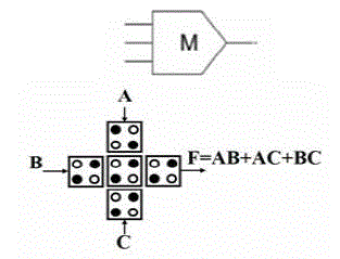
| The governing equation for the majority gate is M (a; b; c) = ab+ bc + ca. Fig. 5 shows the gate symbols and their layouts. Two input AND and OR gates can be implemented with 3 input majority gates by setting one input to a constant. With ANDs, ORs, and inverters, any logic function can be realized. |
| B .QCA Inverter |
| QCA Inverter can be implemented in position QCA cells to invert the output from input logic level. |
CROSSOVER AND MULTILAYER DESIGN
|
| In QCA, there are two crossover options. They are coplanar crossings and multilayer crossovers. It has been believed that single layer designs are possible with QCA because of the ability to create co-planner crossovers. Coplanar crossings require using two cell types (regular and rotated). The regular cell and the rotated cell do not interact with each other when they properly aligned, so rotated cells can be used for coplanar wire crossing. They have very little mutual interaction. In the coplanar crossing, rotated cells are used when two wires cross. In a coplanar crossing, there is a possibility of a loose binding of the signal which causes a discontinuity of the signal propagation and there is the possibility of back-propagation from the far side constant input. So putting enough clock zones between the regular cells across the rotated cells is required. So the complex circuits using coplanar crossover are very likely fail. As well, the crossover is extremely sensitive to fabrication errors and depends on the ability to fabricate two types of QCA cells. Therefore is presented a solution to this Problem. |
CIRCUIT IMPLEMENTATION
|
| The QCA full adder design is shown in Fig. 8.The QCA ring counter design is shown in Fig. 10.The QCA T FlipFlop design is shown in Fig. 12 proposed QCA multiplexor has been designed and simulated using the QCA Designer tool. This tool allows users to do a custom layout and then verify QCA circuit functionality by simulations. It includes two different simulations engines such as a bistable approximation and a coherence vector. The current QCA technology does not specifically set the possible operating frequency and actual propagation delays. Thus, the maximum cell count can be set as a design parameter [6]. |
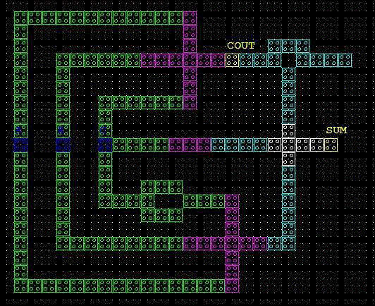
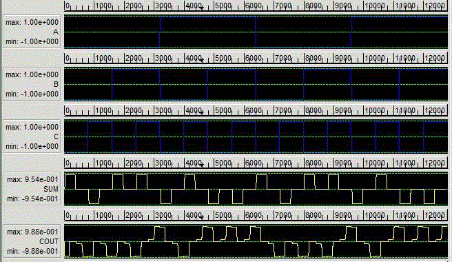
| A full adder is a combinational circuit that forms the arithmetic sum of three input bits. Two of the input variables, denoted by a and b, represent the two significant bits to be added. The third input c,represents the carry from the previous lower significant position. The QCA design of full adder is used to three majority gates and two inverters shown in fig.8 and the simulation result is shown in fig.9. |
| Expression of full adder: |
| Sum = a’b’c + a’bc’+ ab’c’+ abc = majority[ majority(a,b,c)’, majority(a,b,c’),c] |
| Carry = ab+bc+ca = majority(a,b,c) |
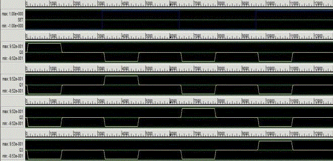
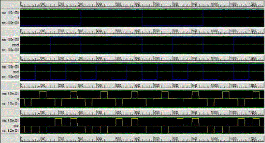
| The 4-bit QCA ring counter design is shown in Fig.10. As it was said, every different subsequent four clockzones is repeated alternatively and operates as a D-FF. It is necessary that D-FF3 output shift to D-FF0 after every clock cycle. So, feedback path only includes a complete clock cycle, and the simulation output is show in fig.11. |
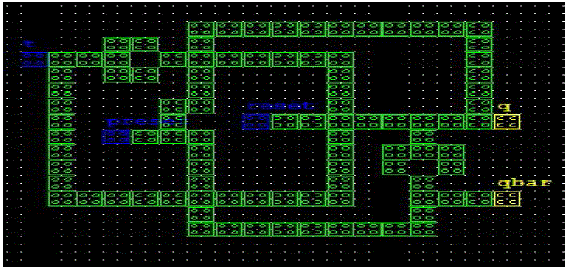
| The T flip-flop changes its output on each clock edge, giving an output on each which if half the frequency of the signal to the T input. The T flip-flop isconstructing from the JK flip-flop. The QCA design of T flip-flop is used to design the three majority gates and two inverters shown in fig.12,and the simulation output is shown in fig.14. |
SIMULATION
|
| With QCA Designer ver.2.0.3, the circuit functionality is verified. The input and output waveforms are shown in Fig. 9, Fig.11, Fig.13 According to QCA Designer, this design has 124 cells (including input and output cells) and an area of approximately 0.25μm2 (each cell is18nm×18nm , with a 2nm gap between cells). |
CONCLUSION
|
| This paper presents design for QCA full adder, full subtractor, ring counter, T flip flop. The layout is done using QCA Designer and this design is analysed according to the complexity and area. Simulation shows that occupied area for this design is 0.25m. For future work, the design can be optimized in terms of complexity and the number of clock zones. Also, computation time and power consumption can be computed for designing. |
Figures at a glance
|
 |
 |
 |
 |
 |
| Figure 1 |
Figure 2 |
Figure 3 |
Figure 4 |
Figure 5 |
|
 |
 |
 |
 |
| Figure 6 |
Figure 7 |
Figure 8 |
Figure 9 |
|
 |
 |
 |
 |
| Figure 10 |
Figure 11 |
Figure 12 |
Figure 13 |
|
References
|
- A.O. Orlov, I. Amlani, G.H. Bernstein, C.S. Lent, G.L. Snider, “Realization of a Functional Cell for Quantum-Dot Cellular Automata,” Science, Vol 277, pp 928-930, 1997.
- P.D. Tougaw and C.S. Lent, “Logical devices implemented using quantum cellular automata,” Journal of Applied Physics, 75:1818, 1994.
- C. S. Lent and B. Isaksen, “Clocked molecular quantum-dot cellular automata,” IEEE Trans. on Electron Dev., 50(9): 1890– 1895, September 2003.
- Kyosun Kim, Kaijie Wu, and Ramesh Karri, “The Robust QCA Adder Designs Using Composable QCA Building Blocks ,” IEEE Trans. On Computer-Aided Design of Integrated Circuits and System, Vol. 26, no. 1, pp. 176-183, January 2007.
- H. Cho, E.E. Swartzlander, “Adder Designs and Analyses for Quantum-Dot Cellular Automata,” IEEE Trans. On Nanotechnology, Vol. 6, no. 3, May 2007.
- M.A. Amiri, M. Mahdavi, S. Mirzakuchaki, “QCA Implementation of a MUX-Based FPGA CLB”, ICONN 2008, pp. 141–144.186 [7]Himanshu Thapliyal, Student Member, IEEE, and Nagarajan Ranganathan, Fellow, IEEE, “Reversible Logic-Based Concurrently Testable Latches for Molecular QCA“IEEE Transactions On Nanotechnology, VOL. 9, NO. 1, January 2010.
|