Keywords
|
| Resonant tunnelling diode, transmission coefficient, double barrier, Gallium Arsenide, resonant energy |
INTRODUCTION
|
| Semiconductor devices own various advantages in terms of performance and functionality. Nano- devices carry charge and excitons efficiently, and are ideal building blocks for nanoscale electronics and optoelectronics. During recent times, there has been incredible development made to explore the novel nanotechnology for future nanoelectronic applications [1]. There are several types of p–n junction diodes that either emphasizes different physical aspects of a diode by geometric scaling, doping level, choosing the right electrodes, are just an application of a diode in a special circuit, or are really different devices like the Gunn and laser diode. In particular, several emerging nanoelectronic devices such as field-effect transistors (FETs), nanowire FETs, and planar III–V compound semiconductors grasp promise as potential devices to be integrated enhancing circuit functionality. Recently, the impressive developments of high brightness gallium arsenide (GaAs)-based light-emitting diodes (LEDs) have made it possible for LEDs to be implanted in large size flat-panel displays [2-7]. Such incorporated LED backlight modules allow the images to be much sharper and more colorful. To quickly penetrate the consumer display market with LEDbased solutions, there is a great need to improve the internal as well as external quantum efficiency in order to increase their light output power and to reduce the total cost of the LED modules. However, the external quantum efficiency of GaN-based LEDs is generally low, because the refractive index difference between the nitride epitaxial material and the air environment is high [8] [9]. The elements from the Group III-V materials possess a significant contribution and their applications have attracted the researchers to investigate their potential use in optoelectronic devices, such as light emitting diodes (LEDs) and laser diodes (LDs). Several contributors demonstrated their application as various electronic gadgets such as displays, traffic signals, backlights for cell phones, lighting indicators and printers. Inspite of these two types of diodes, tunnel diode came into existence and in short span of time becomes an essential microwave device [10-15]. The resonant tunneling diode (RTD) belongs to the family of these diodes and is believed to be an element of a future low power, high density integrated circuit because of a possible ultra low power operation with a few electrons. |
| Several researchers have already been reported different techniques of modelling and synthesis of diodes using nanostructures. The techniques used for fabrication includes lithography, chemical electrodeposition technique, sol-gel method, spin coating and many more. For modelling, several researchers have shown their reliability on some trusted softwares like, ANSYS, COMSOL MULTIPHYSICS, CoventorWare, PSpice and some online simulators like NANOHUB. The diodes were designed by taking unique nanostructure like, nanowires, nano-films and carbon nano tubes (CNT). For the practical application, it is necessary for RTD to be operated at room temperature. In this regard, two different analytic models of RTD’s for double barrier are simulated by altering the dimensions of the device. Hence, in this paper, 2B RTD’s are designed to evaluate their performances. |
METHODOLOGY
|
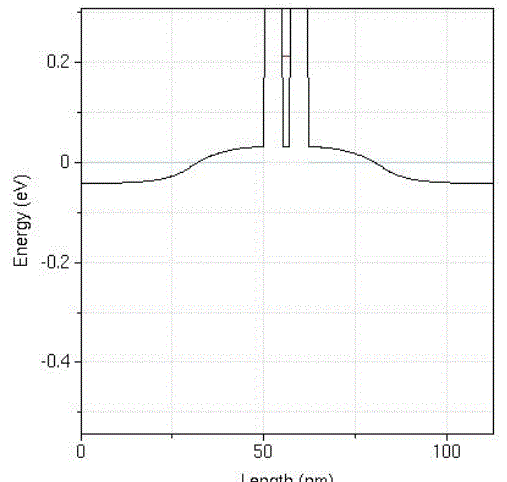
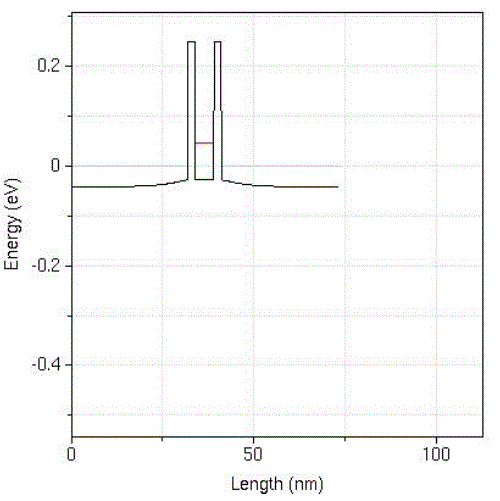
| The models are designed for double barrier Resonant tunnelling diode has been simulated at room temperature. The selected material for simulation is GaAs with AlGaAs as barriers. The metal contacts used are Aluminium (Al). The layout for different dimensional aspects for double barrier resonant tunnelling diodes is shown in fig.1 and fig. 2 respectively. |
| From fig. 1 and fig. 2, it is clear that the total length of the device is 112 nm and 73 nm, respectively. The applied biasing voltage is set at 0.5 volts. Different doping concentrations are selected in different zones of the device. The doping profile for both the devices is same and is shown in table 1. |
| The input parameters of the device is adjusted and optimized as is shown in table 2. These parameters are important for the successful evaluation of the device. |
RESULTS AND DISCUSSIONS
|
| The simulated results for the double barrier resonant tunnelling diodes are taken using effective mass model. Fig. 3 shows the conduction band of double barrier resonant tunnelling diode with thinner well width where as fig. 4 shows the conduction band for double barrier resonant tunnelling diode having wider well width. |
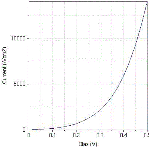
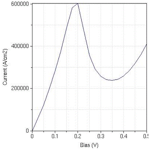
| The conduction peak of these RTD occurs when a localized state in the emitter notch region is aligned with the well state. Similarly, Fig. 5 shows the current vs voltage characteristics for double barrier resonant tunnelling diode with small well width while fig. 6 for double barrier resonant tunnelling diode for longer well width. |
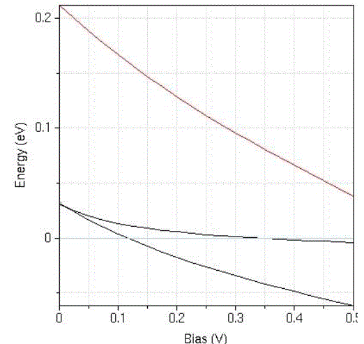
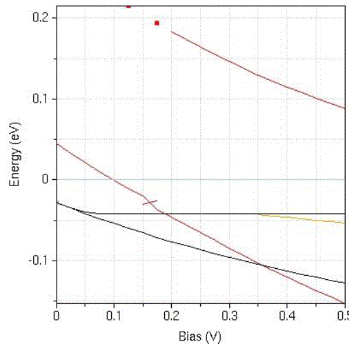
| Both the VI characteristics differ due to difference in structural design used. For thinner well width of double barrier RTD, the forward VI characteristics are almost same as that of simple pn junction diode. However, for longer well width of double barrier RTD, the current increases with respect to voltage upto the peak point. After peak point, the device shows negative resistance region upto the valley point. For a specific voltage range, the current is a decreasing function of voltage. This property is very important in the circuit implementation because it can provide for the different voltage-controlled logic states corresponding to the peak and valley currents. Fig. 7 and fig. 8 shows the resonant energies for single and double barrier RTD respectively. |
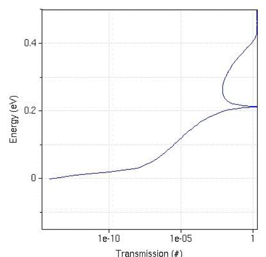
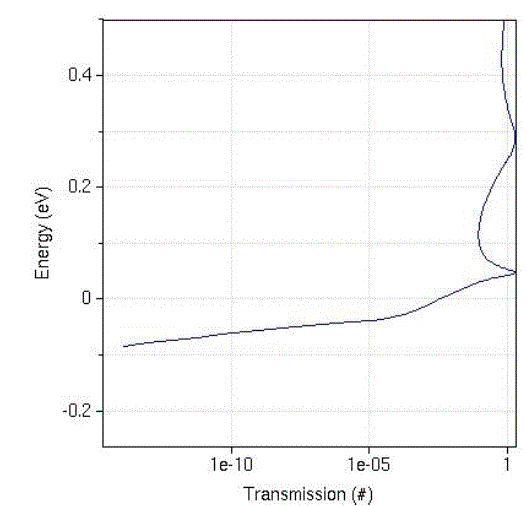
| Resonances occur when the electron wavelength is a half integer multiple of the well width. The resonance locations are given by the energies corresponding to these wavelengths on the energy dispersion relationship. Band nonparabolicity reduces the dispersion for a given value of k. Therefore, for both the models, the region between the two barriers acts as a quantum well with discrete energy states. Resonant tunnelling through the double-barrier structure occurs when the energy of the electrons flowing from the source coincides with one of the discrete energy levels in the well. The position of the bounded states within the well can be modulated with a gate bias. Fig. 9 shows the transmission coefficient for single barrier resonant tunnelling diode while fig. 10 for double barrier resonant tunnelling diode. |
| Tunnelling of electrons depends on the barrier width. For both the RTD’s the transmission coefficients become nearly equal to unity due to lower quantized energy level. The value of transmission coefficients depends on the barrier width and applied electric field. Since for both the simulated RTD’s, electric field and the barrier widths are same, hence the transmission coefficients for both are almost same. |
CONCLUSION
|
| In this work, analytic model of different double barrier RTD’s are simulated by taking different dimensions of the device. It can be concluded that the double barrier RTD with wider well shows better performance for high power signals and can be used as oscillator, whereas the double barrier RTD with wider well width shows better performance as low power device. For both the structures, the value of transmission coefficients reaches unity when resonance occurs. It can also be concluded that resonance peaks are split into number of small peaks and the number of small peaks is generally equal to the number of barriers. Also, the absence of applied field is preferred to achieve maximum transmission coefficient. |
| |
Tables at a glance
|
 |
 |
| Table 1 |
Table 2 |
|
| |
Figures at a glance
|
 |
 |
 |
 |
 |
| Figure 1 |
Figure 2 |
Figure 3 |
Figure 4 |
Figure 5 |
|
 |
 |
 |
 |
 |
| Figure 6 |
Figure 7 |
Figure 8 |
Figure 9 |
Figure 10 |
|
| |
References
|
- Mike Tooley, Electronic Circuits: Fundamentals and Applications, 3rd Ed. Routlege, ISBN 1-136-40731-6, 2012.
- S. M. Sze, Physics of Semiconductor Devices, Wiley Publications, 2002.
- R. L. Batdorf , A. G. Chynoweth , G. C. Dacey and P. W. Foy, ‘Uniform silicon P-N junctions. I. Broad area breakdown’, J. Appl. Phys.,vol. 31, pp.1153 -1160, 1960.
- A.M. Song, M. Missous, P. Omling, A.R. Peaker, L. Samuelson, and W. Seifert, ‘Unidirectional electron flow in a nanometer-scalesemiconductor channel: A self-switching device’, Appl. Phys. Lett., vol. 83, pp. 1881-1883, 2003.
- J. O. Wesström, ‘Self-gating effect in the electron Y-branch switch’, Phys. Rev. Lett., vol. 82, pp. 2564-2567, 1999.
- A. M. Song, ‘Formalism of nonlinear transport in mesoscopic conductors’, Phys. Rev. B, vol. 59, pp. 9806-9809, 1999.
- J. Mateos, B.G. Vasallo, D. Pardo, T. González, E. Pichonat, J. S. Galloo, S. Bollaert, Y. Roelens and A. Cappy, ‘Non-linear effects in Tbranchjunctions’, IEEE Electron Device Letters, vol. 51, pp. 521-523, 2004.
- T. Gonzalez, B.G. Vasallo, D. Pardo and J. Mateos, ‘Room temperature nonlinear transport in ballistic nanodevices’, SemiconductorScience and Technology, vol. 19, pp. S125-S127, 2004.
- B.G. Vasallo, T. González, D. Pardo and J. Mateos, ‘Monte Carlo analysis of four-terminal ballistic rectifiers’, Nanotechnology, vol. 15,pp. S250-S253, 2004.
- A. J. Heeger, ‘Light emission from semiconducting polymers: Light-emitting diodes, light-emitting electrochemical cells, lasers and whitelight for the future’, Solid State Commun., vol. 107, pp 673-679, 1998.
- H. C. J. Lutz, H. Schlangenotto, U. Scheuermann, I. De Doncker, Semiconductor Power Devices, pp 159-224, 2011.
- G. R. Liang, T. H. Cui and K. Varahramyan , ‘Fabrication and electrical characteristics of polymer-based Schottky diode’, Solid StateElectronic, vol. 47, pp. 691-694, 2003.
- R. L. Batdorf , A. G. Chynoweth , G. C. Dacey and P. W. Foy, ‘Uniform silicon P-N junctions. I. Broad area breakdown’, J. Appl. Phys.,vol. 31, pp.1153 -1160, 1960.
- L. Esaki, ‘Long journey into tunneling’, in Proc. IEEE, vol. 62, pp.825-830, 1974.
- nanoHUB.org., ‘Advancing Education and Research in Nanotechnology’, Computing in Science & Engineering, vol. 10, pp.17-23, 2008.
|