International Journal of Innovative Research in Science, Engineering and Technology
ISSN ONLINE(2319-8753)PRINT(2347-6710)
ISSN ONLINE(2319-8753)PRINT(2347-6710)
Trupti Patel1, G.K. Solanki2, Vimal S. Joshi 3
|
| Related article at Pubmed, Scholar Google |
Visit for more related articles at International Journal of Innovative Research in Science, Engineering and Technology
Among the IV-VI semiconductor compounds, Tin sulphide (SnS), Tin selenide (SnSe), Germanium Sulphide (GeS) and Germanium Selenide (GeSe) have the layered orthorhombic structure with eight atoms per unit cell forming biplanar layers normal to the largest c axis [1-4]. In the present work, investigation on growth of single crystals of SnSeRex (x = 0, 0.1, 0.2, 0.3, 0.4) by direct vapour transport technique (DVT) using two zone horizontal furnace is reported. Confirmation of stoichiometric proportion of constituent elements and determination of crystal structure of grown crystals is done by Energy Dispersive Analysis of X-rays (EDAX).The structural behaviour was accomplished by X-Ray diffraction (XRD) studies. As a result, it seen to be orthorhombic structure and results are discussed.
Keywords |
| Semiconducting IV-VI compounds, growth from vapour, EDAX and XRD analysis |
INTRODUCTION |
| During recent years, science and technology enjoy a higher degree of sophistication due to the availability of high quality materials. The layered compounds with a distorted rock salt structure of the orthorhombic space group; among the binary IV-VI semiconductor compounds are tin sulphide (SnS), tin selenide (SnSe), germanium sulphide (GeS) and germanium selenide (GeSe) [1,5,6]. These compounds are also known as lamellar semiconductors which attracted considerable attention because of their important specific properties in the field of optoelectronics [7], holographic recording systems [8], electronic switching [9-10] and infrared production and detection. Moreover SnSe is a semiconductor with a band gap of about 1 eV having a potential as an efficient solar cell material [11-12]. It is clear from that the literature survey that a lot of research work has been done on Tin Selenide single crystal; however, the work on compounds Tin Selenide with substitution of transition metal is almost negligible. Hence, it was decided to work on SnSeRex (x = 0, 0.1, 0.2, 0.3, 0.4) compounds by direct vapour transport technique (DVT) using two zone horizontal furnace. The results are described in the paper. |
EXPERIMENTAL TECHNIQUE |
| CRYSTAL GROWTH |
| In present investigations, crystal growth of SnSeRe family was done by direct vapour transport technique using dual zone horizontal furnace. The furnace was constructed by University Science and Instrumentation Centre (USIC), Sardar Patel University by using a special sillimanite threaded tube closed at one end, 450 mm in length, 70 mm outer diameter, 56 mm inner diameter with threaded pitch of 3 mm, imported from koppers Fabriken Feuerfester, Germany. The furnace was controlled by a microcontroller with thermal profile programming facility. High quality quartz ampoules were used for crystal growth which having dimensions of 24 cm length, 2.4 cm outer diameter and 2.2 cm inner diameter. Firstly boiled water was used to wash the ampoule after then with hot mixture of concentrated HNO3 and H2So4 taken in equal proportion, followed by washing of ampoule with distilled water. Then ampoule was filled with concentrated HF and heated until whole HF evaporated, so that the inner surface of the ampoule become rough which enhances the nucleation process during the growth. At the end this ampoule was washed by double distilled water at least 8 to 10 times. A cleaned ampoule was kept in oven for nearly 24 hour to make it moisture free. Highly pure powder of Sn (99.99%), Se (99.99%) and Re (99.99%) were taken in a stoichiometric proportion in the ampoule for the compound preparation. It was evacuated to a 10-5Torr and then sealed. The sufficient care was taken for vigorous shaking so as to distribute the mixture along the length uniformly. The ampoule was set in a horizontal furnace. Its temperature was slowly raised till it reaches to 1073 K. It was maintained at this temperature for a period of 3 day for charge preparation. The ampoule was then slowly cooled and brought to room temperature. The resulting free flowing shiny homogeneous polycrystalline powder was achieved. This charged ampoule was placed in a dual zone horizontal furnace. For different member of the series the temperatures of hot zone and cold zone of the ampoule were kept as shown in Table 1. Finally resulting crystals were collected from the ampoule. The appropriate growth conditions for all samples are reported in Table 1. |
 |
| STRUCTURAL CHARACTERIZATION |
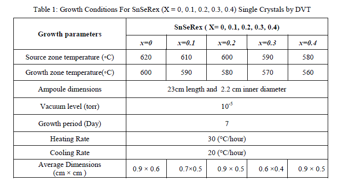
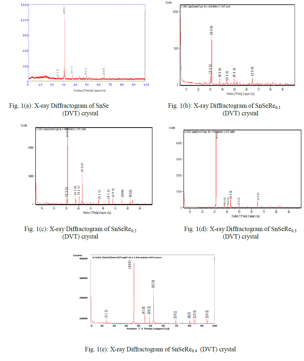
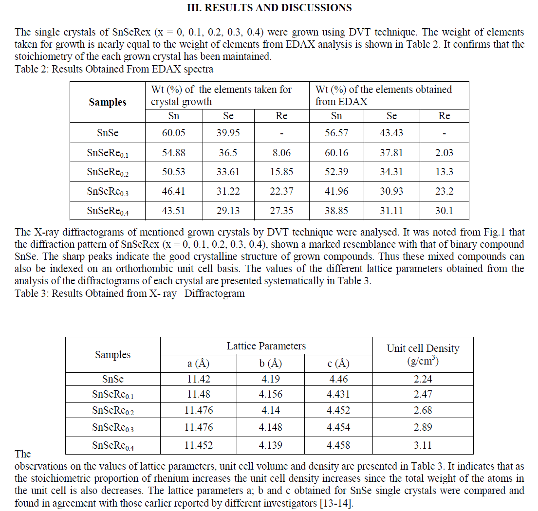
| In present case, the grown crystals have been characterized for their structural propertied using EDAX and XRD techniques. The chemical proportions of elements in grown crystals are obtained from the Energy Dispersive Analysis of X-rays (EDAX) which has been done at kalabhavan, M. S. University, Baroda. The energy dispersive analysis using Xrays (EDAX) experiment has been carried out on each grown sample for the determination of the stoichiometric proportion of Sn, Se and Re. The X–ray diffractograms were obtained for each sample with Philips X-ray diffractometer PW 1820 employing CuKα radiation. The powder obtained during the growth process for each sample was prepared for the X-ray diffraction study experiment. The lattice parameters, hkl reflections and d spacing of the grown crystals were determined by comparison with JCPDS data as well as by using power X software. The X-ray diffraction patterns obtained for SnSeRex (x = 0, 0.1, 0.2, 0.3, 0.4) are shown in Fig. 1 (a), (b), (c), (d) and (e) respectively. |
 |
 |
ACKNOWLEDGEMENT |
| The authors are thankful to Department of Physics, Sardar Patel University, Vallabh Vidyanagar and M. S. University of Baroda for carrying out some part of this work. Corresponding author Vimal Joshi is thankful to the University Grants Commission, New Delhi for Financial Assistance under Minor Research Project Scheme. The authors are also grateful to Prof. U. H. Patel for their valued guidance and support. The authors are also thankful to Petlad Education Trust for motivation. |
References |
|