International Journal of Innovative Research in Science, Engineering and Technology
ISSN ONLINE(2319-8753)PRINT(2347-6710)
ISSN ONLINE(2319-8753)PRINT(2347-6710)
1N.Bhuvaneswari, 2V.Gowrishankar, 3Dr.K.Venkatachalam
|
Visit for more related articles at International Journal of Innovative Research in Science, Engineering and Technology
In this paper, we present a performance comparison of dynamic comparators. As delay is directly correlated with the submicron scaling, we investigate the performance of the above comparators in terms of delay and Power-Delay Product (PDP). PDP gives the average energy dissipated by the comparator for a single comparison. Simulation results using Tanner EDA revealed better performance of High Speed Dynamic Comparator (HSDC) compared to conventional clocked comparators in 180nm, 250nm and 350nm technologies. Implementation results reveal that high speed dynamic comparator has energy dissipation compared to the best of the designs used for comparison in 180nm technology, when operated at 50 MHz.
Keywords |
| Ultra Deep Sub Micrometer (UDSM),Dynamic Comparator, Flash ADCs, Common Mode Voltage. |
INTRODUCTION |
| Nowadays high speed devices like High speed ADCs, Comparator became of great importance. And for these high speed applications, a major thrust is given towards low power methodologies. Minimization in power consumption in these devices can be achieved by moving towards smaller feature size processes. However, as we move towards smaller feature size processes, the process variations and other non idealities will greatly affect the overall performance of the device. The performance limiting blocks in such ADCs are typically interstage gain amplifiers and comparators.The power consumption, speed takes major roll on performance measurement of ADCs. Comparators are known as 1-bit analog to digital converter and for that reason they are mostly used in large abundance in A/D converter. The basic functionality of a CMOS comparator is used to find out whether a signal is greater or smaller than zero or to compare an inputsignal with a reference signal and outputs a binary signal based on comparison.Many high speed ADCs, such as flash ADCs, require high-speed, low-power comparator. Due to high speed, low power consumption, high input impedance and full-swing output dynamic latched comparators are very attractive. They use positive feedback mechanism with one pair of back-toback cross coupled inverters (latch) in order to convert a small input-voltage difference to a full-scale digital level in a short time. Designing high-speed comparators suitable to be operable in low supply voltages is a more challenging work. Many techniques, such as supply boosting methods [2] that can handle higher supply voltages have been developed to meet low-power design challenges. These are effective but introduces reliability issues in CMOS technologies. Two power-saving schemes namely the current-controlled latch sense amplifier and static power-saving input buffer (SPSIB) for high-performance VLSIs with a large-scale memory and many interface signals were described by Kobayashi et al [7]. A CMOS latch-type voltage sense amplifier was designed with a separated input and cross-coupled stage [4]. Based on Blalock [8] approach, a 1-bit quantizer for sub-1V ΣΔ modulators was proposed by Maymandi-Nejad and Sachdev [9]. |
| A comparator with a modified latch [2] is different from the conventional circuit by replacing a new latch for low power supply voltage operation (i.e.) for supply voltages down to 0.65V for 65nm technology. This latch is helpful in low power supply voltage operation. A low power, low voltage Successive Approximation Analog-to-Digital Converter (SAR ADC) design based on supply boosting technique is proposed in [3]. SBT is suitable for mixed-signal circuit designed for energy limited applications and systems in where supply voltage is in the order of threshold voltages of the process. Many researches contribute in analyzing the performance of the dynamic comparators. Random decision errors are analyzed in the dynamic comparators using LPTV (Linear Periodically Time Varying) model [5]. A method to estimate the input referred noise in fully dynamic regenerative comparators leveraging a reference architecture is proposed in [10]. The effect of load capacitor mismatch on the offset of a regenerative latch comparator is analyzed in [11]. |
| Kickback noise reduction by neutralization technique is investigated by Figueiredo and Vital [12] and offset cancellation by body voltage adjustment using low-power simple analog control feedback circuit without any additional capacitive loading at the comparator output is investigated by Babayan-Mashhadi and Lotfi [13]. A novel balanced method is proposed to facilitate the evaluation of operating points of transistors in a dynamic comparator in [14], making it possible to obtain an explicit expression for offset voltage in dynamic comparators. |
DYNAMIC COMPARATOR DESIGNS |
| Conventional dynamic [7] and double-tail comparators [4], [1] are clocked regenerative comparators which are useful in high speed ADCs like flash ADC because of their fast decision making capability due to strong feedback loop in the regenerative latch. The analyses presented in literature investigate the performance of the comparators in terms of noise [10], offset [11], [13] and [14], random decision errors [5] and kick back noise [12]. Since delay is directly correlated with the submicron technology, we investigate the performance of the above comparators in terms of delay using different technology files. |
| A. Conventional Dynamic Comparator |
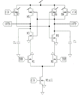
| Kobayashi et al. (1993) [7] proposed a latch type dynamic comparator and is shown in Fig.1 (two cross-coupled inverters).It has high input impedance, rail-to-rail output swing and there is no static power consumption. There exists an indirect influence of the parasitic capacitances of the input transistors (larger gate area for lower offset) to the output nodes and, thus, influences switching speed. The novelty of the Kobayashi’s design is the use of a sleep transistor (Mtail) which establishes the path from VDD to GND only when the circuit is active and the design operates in two phases to produce an output. |
| a) Reset phase:In reset phase CLK=0, sleep transistor Mtail is OFF, and reset transistors (M7–M8) will be ON and pull both output nodes Outn and Outp to VDD to define a start condition and to have a valid logical level during reset. |
| b) Comparison phase:In the second phase i.e., comparison phase CLK=VDD, sleep transistor Mtail is ON and transistors M7 and M8 are OFF. The output voltages (Outp, Outn), which had been pre-charged to VDD, start to discharge in this phase with different discharging rates depending on the corresponding input voltage (INN/INP). Assuming the case where VINP>VINN, Outp discharges faster than Outn, hence when Outp (discharged by transistor M2 drain current), falls down to VDD–|Vthp| before Outn (discharged by transistor M1 drain current), the corresponding pMOS transistor (M5) will turn on initiating the latch regeneration caused by backto- back inverters (M3, M5 and M4, M6). Thus, Outn pulls to VDD and Outp discharges to ground. If VINP<VINN, the circuits works vice versa. The expression for the delay of the conventional dynamic comparator is obtained as |
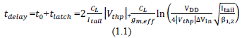 |
 |
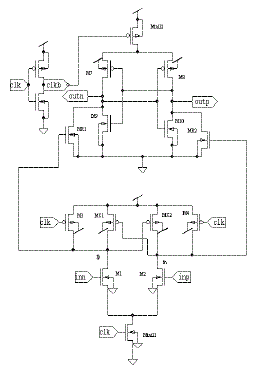
| B. Conventional Double-Tail Dynamic Comparator |
| Shinkel et al. (2007) [4] proposed a double-tail dynamic comparator which has a separate input-gain stage and outputlatch stage and is shown in Figure2. The grouping of input and output stages as two different stages made this comparator to have a lower and more stable offset voltage over a wide common-mode voltage (Vcm) range and to operate at reduced supply voltage. It is because by controlling the sizes of the tail transistors (Mtail1 and Mtail2) of the input and output-stage in such a way that a small tail current for the differential input pair can obtain a long integration time and a better gm/ID ratio for a bigger gain (hence, less offset voltage) and a large tail current for the output latch-stage for fast regeneration, soone can get high speed and low offset voltage with less dependence on Vcm. Since this comparator requires both and signals for its operation, a high synchronization between and is required because the second stage has to detect the voltage difference between the differential outputs of the first gain stage at very limited time. If a simple inverter is used to generate , it inserts an additional load on the clock generator. If is lagging , it results in increased delay and if is leading , it results in increased power dissipation due to existence of short circuit current path Mtail2 to M7/M8 through MR1/MR2 and it can even increase the latch offset voltage if the device mismatch between M7 and M8 is significant. |
| Similar to Kobayashi et al.’s (1993) design Shinkel et al’s (2007) comparator has two phases of operation viz., reset phase and comparison phase, to compare the inputs. |
| a) Reset phase:In this phase CLK=0, Mtail1, and Mtail2 are OFF, transistors M3-M4 pre-charge fn and fp nodes to VDD, which in turn causes transistors MR1 and MR2 to discharge the output nodes to ground. |
| b) Comparison Phase : In this phase CLK = VDD, Mtail1 and Mtail2 turn on, M3-M4 turn off and voltages at nodes fn and fp start to drop with the rate defined by IMtail1/Cfn(p) and on top of this, an input-dependent differential voltage ΔVfn(p) will build up. The intermediate stage formed by MR1 and MR2 passes ΔVfn(p) to the cross coupled inverters and also provides a good shielding between input and output, resulting in reduced value of kickback noise. However in Shinkel et al’s (2007) comparator both intermediate transistors will be cut-off, (since fn and fp nodes both discharge to the ground) and thus, during reset phase, these nodes have to be charged from ground to VDD, which leads to high power consumption. The expression for the delay of the conventional double tail comparator is obtained as |
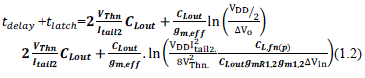 |
 |
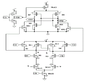
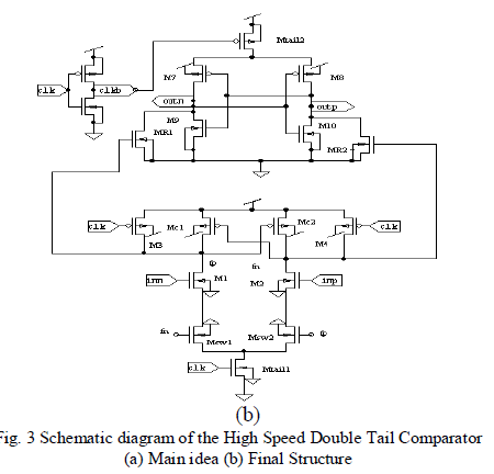
| C. High Speed Double-Tail Dynamic Comparator |
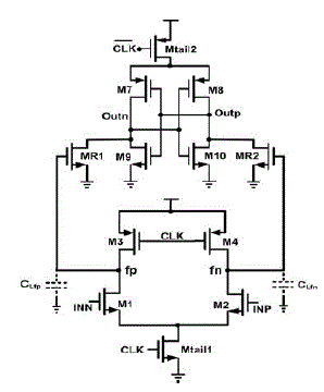
| SamanehBabayan-Mashhadi and Reza Lotfi (2013) [1] proposed a high speed energy efficient double-tail dynamic comparator. Due to the better performance of double-tail architecture in low-voltage applications, SamanehBabayan- Mashhadi and Reza Lotfi design incorporates double-tail in its architecture. The main idea of this comparator is to increase ΔVfn/fp in order to increase the latch regeneration speed. For this purpose, two control transistors (Mc1 and Mc2) have been added to the first stage in parallel to M3/M4 transistors but in a cross-coupled manner as shown in Figure3. The design operates in two phases to compare the two inputs viz., Reset Phase and Comparison Phase. |
| a) Reset phase : In reset phase (CLK=0, Mtail1 and Mtail2 are OFF, avoiding static power), M3 and M4 pulls both fn and fp nodes to VDD, hence transistor Mc1 and Mc2 are cut off. Intermediate stage transistors, MR1 and MR2, reset both latch outputs to ground. |
| b) Comparison Phase :In this phase (CLK=VDD, Mtail1, and Mtail2 are ON), transistors M3 and M4 turn OFF. Furthermore, at the beginning of this phase, the control transistors are still OFF (since fn and fp are about VDD). Thus, fn and fp start to drop with different rates according to the input voltages. Suppose VINP >VINN, thus fn drops faster than fp, (since M2 provides more current than M1). As long as fn continues falling, the corresponding pMOS control transistor (Mc1 in this case) starts to turn on, pulling fp node back to the VDD; and another control transistor (Mc2) remains off, allowing fn to be discharged completely. The total delay of the proposed comparator is achieved from |
 |
| 1) Static Power Eliminated version (HSDC -SPEV): To overcome the issue of direct current path from VDD to ground two nMOS switches below the input transistors [Msw1 and Msw2] and is shown in Fig. 4. At the beginning of the decision making phase, due to the fact that both fn and fp nodes have been pre-charged to VDD (during the reset phase), both switches are closed and fn and fp start to drop with different discharging rates. As soon as the comparator detects that one of the fn/fp nodes is discharging faster, control transistors will act in a way to increase their voltage difference. Suppose that fp is pulling up to the VDD and fn should be discharged completely, hence the switch in the charging path of fp will be opened (in order to prevent any current drawn fromVDD) but the other switch connected to fn will be closed to allow the complete discharge of fn node. |
 |
 |
| In other words, the operation of the control transistors with the switches emulates the operation of the latch. The novelty of the design is that it has high speed compared to the conventional double-tail dynamic comparator [4] due to high initial output voltage difference (ΔVo) and Effective transconductance (gmeff). |
RESULT ANALYSIS |
| Transient simulation of the conventional dynamic comparator [7], conventional double-tail comparator [4] and High speed Energy efficient double-tail comparator [1] were performed using mentor graphics with 180nm sub-micron technology file. The pMOS and nMOS transistors in the circuits are sized to satisfy its drive capability. In order to measure the delay at the output nodes, CLK signal is set as the reference. The delay at the output nodes (Outn and Outp) are measured with respect to the clock. The parameters used for the simulation are: ΔVin=5mV, Vcm=0.7V, VDD=0.8V,INN=0.6975V and INP=0.7025V with the rise and fall time of the clock maintained equal and is kept at 1ns. Here the results of the existing comparators in terms of delay, power and PDP are shown in TABLE I for the frequency of 50MHz. It is seen from TABLE I that the delay of the HSDC is lower better compared to Kobayashi’s [7] and Shinkel et al’s [4] designs respectively. This is because the HSDC enhances the speed by Enhancing the latch output voltage difference at time t0 i.e., (ΔV0) and by Enhancing the latch effective transconductance (gm,eff). |
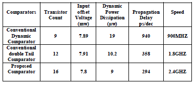 |
| The enhanced speed of the HSDC design shows better delay reduction compared to conventional dynamic comparators. The number of transistors is more in the high speed energy efficient design compared to the conventional designs. |
CONCLUSION |
| A performance comparison of existing clocked dynamic comparators in different scaling technologies is carried out in this brief. As high speed and minimum energy dissipation are the main criteria in day to day portable applications, we performed an extensive delay analysis of the comparators mentioned in literature. Experimental evaluation of the existing comparator designs shows that the HSDC design show better delay reduction compared to conventional dynamic comparator designs. The analysis reveals the suitability of HSDC designs for high speed ADCs like flash ADC used in portable devices. |
References |
|