Keywords
|
| C2CMOS, 22nm technology, Power dissipation, Propagation delay |
INTRODUCTION
|
| For high performance VLSI chip-design, the choice of the back-end methodology has a significant impact on the design time and the design cost. Latches and flip-flops have a direct impact on power consumption and speed of VLSI systems. Therefore various following flip flop topologies were designed for some dedicated applications. |
| A flip-flop is bistablemultivibrator . The circuit can be made to change state by signals applied to one or more control inputs and will have one or two outputs. It is the basic storage element in sequential logic. Flip-flops and latches are a fundamental building block of digital electronic systems used in computers, communications, and many other types of systems. |
| Flip-flops and latches are used as data storage elements. Such data storage can be used for storage of state, and such a circuit is described as sequential logic. When used in a finite-state machine, the output and next state depend not only on its current input, but also on its current state (and hence, previous inputs). It can also be used for counting of pulses, and for synchronizing variably-timed input signals to some reference timing signal. |
| Flip-flops can be either simple (transparent or opaque) or clocked (synchronous or edge-triggered); the simple ones are commonly called latches. The word latch is mainly used for storage elements, while clocked devices are described as flip-flops. A latch is level-sensitive, whereas a flip-flop is edge-sensitive. That is, when a latch is enabled it becomes transparent, while a flip flop's output only changes on a single type (positive going or negative going) of clock edge. |
| In digital CMOS circuits there are three sources of power dissipation, the first is due to signal transition, the second comes from short circuit current which flows directly from supply to ground terminal and the last is due to leakage currents. As technology scales down the short circuit power becomes comparable to dynamic power dissipation. Furthermore, the leakage power also becomes highly significant. High leakage current is becoming a significant contributor to power dissipation of CMOS circuits as threshold voltage, channel length and gate oxide thickness are reduced. When technology scales down, total power dissipation will decrease and at the same time delay varies depends upon supply voltage, threshold voltage, aspect ratio, oxide thickness, load capacitance. |
RELATED WORK
|
| Design of Flip-Flops for High Performance VLSI Applications using Deep Submicron CMOS Technology Rishikesh V. Tambat?*and SonalA.Lakhotiya??Electronics& Telecommunication, G.H. Raisoni College of Engg, Amravati, India. Accepted 01 April 2014, Available online 10 April 2014, Vol.4, No.2 (April 2014) |
| In this paper, an exhaustive analysis and design methodology for commonly used high-speed flip-flops topologies in 90nm CMOS technologies has been carried out. The comparison has been performed with area, delay and power dissipation. The impact of layout parasitic has been included in the transistor-level design phase. The flip-flops chosen for a thorough comparative analysis, whose results are reported in result section. According to the presented results, the fastest topology are the C2CMOS and DET since the delay, with respect to area and number of transistor count TSPC and C2CMOS are better while with respect to power dissipation SET shows better result, the best lowpower flip-flops are the SET. Moreover, the best topology under clock skew and less propagation delay are DET and C2CMOS. |
| They conclude that efficient design architecture based on power dissipation, propagation delay and transistor counts for portable applications are TSPC, SET, DET and C2CMOS Flip-flop. Considerate the suitability of flip-flops and selecting the best topology for a given application is an important issue; the low power design SET is suitable for portable applications. |
| Above performance comparison shows that the C2CMOS and TSPC flip flop architecture shows better result on given key parameters compared with SET and DET. This means that both architectures are suitable in low power, fast switching and minimum area applications. |
PROPOSED ALGORITHM
|
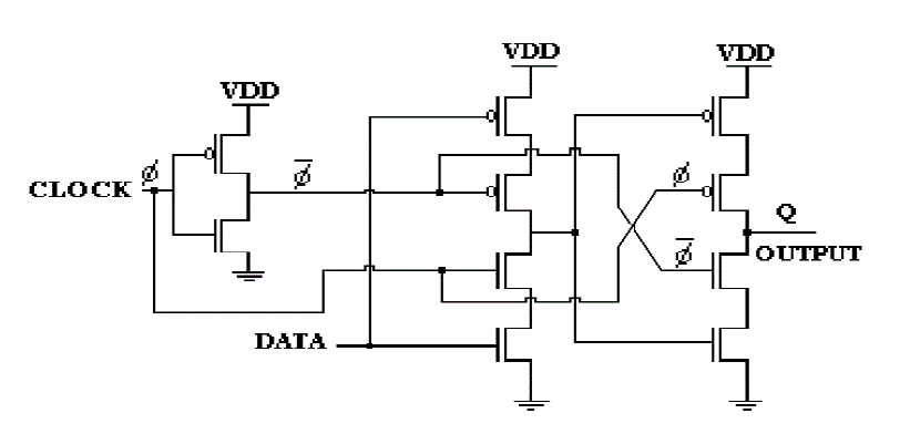
| An ingenious negative edge-triggered register that is based on a master-slave concept insensitive to clock overlap is shown in figure 1. This circuit is called the C2CMOS (Clocked CMOS) flip-flop which operates in two phases: when clk=1, the first driver is turned on, and the master stage acts as an inverter sampling the inverted version of D. The master stage is in the evaluation mode. When clk=0, the master stage section is in hold mode, while the second section evaluates. The previous value stored is propagated to the output node through the slave stage, which acts as an inverter. |
| The above circuit diagram is of clock 2 CMOS flip flop topologies in that the data signal is applied to upper PMOS transistors lower NMOS transistor of the first stage of flip flop, clock signal Ø is applied to NMOS of first stage & PMOS transistor of second stage of circuit and its inverted clock signal is applied to PMOS transistor of first stage & NMOS transistor of second stage. The output of the first stage is applied as input to the second stage of architecture the Output of C2CMOS flip flop is getting at the node „Q?. |
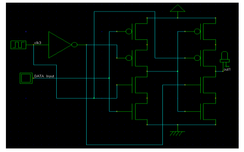
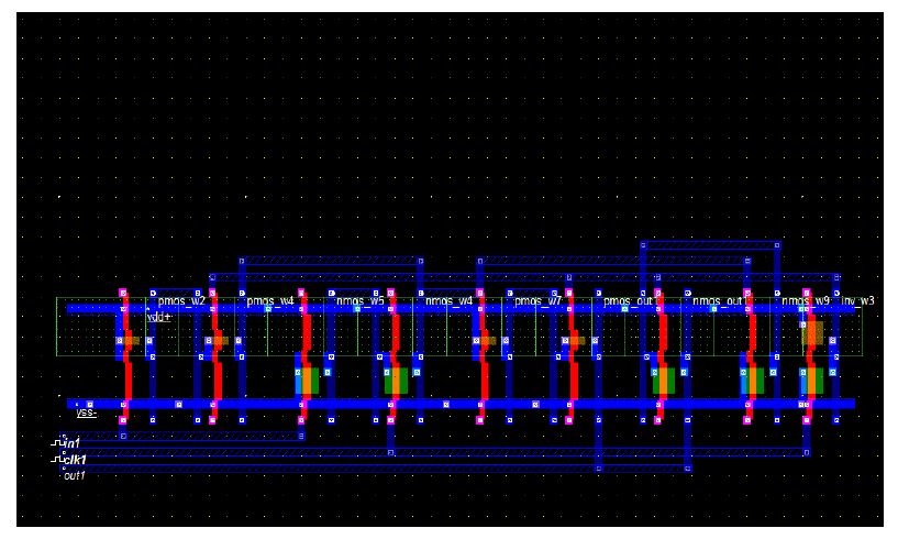
| Above schematic of C2CMOS flip flop is drawn in layout structure with the help of Microwind simulation tool. When the input D is „1? and clock is „1? then master stage is ON & slave is OFF, when input D is „0? and clock is „0? then master stage is OFF & slave is ON |
| In above C2MOS layout design we used only three metal layers and the complete design required only 10 transistors which is less as compares with other. |
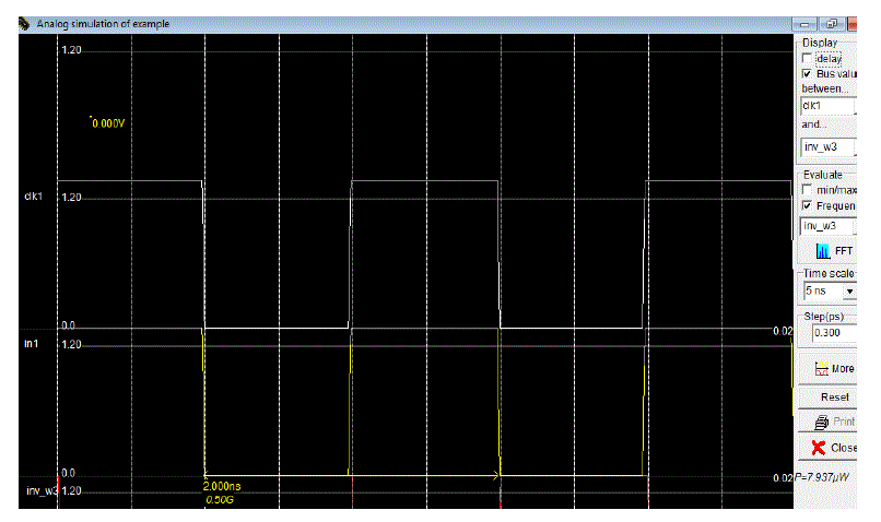
| Simulation output of the C2CMOS flip flop as shown in above figure 4. From the simulation it clear that the output „Q? follows the input „D? at negative (falling) edge of the clock. The total power required by the C2CMOS flip flop is near 8μw is very low as compared with other architectures, it operates on 1.2V and the propagation delay is of 5ps. |
CONCLUSION
|
| One of the most serious problems in VLSI circuit is the area, power dissipation and propogation delay. The Flip-Flop design using C2CMOS architecture with 22nm technology decreases the power dissipation and propogation delay of the Flip-Flop compared with the 90nm technology. C2CMOS with 90nm had 11μw power dissipation and 6ps delay but 22nm C2CMOS has only 8μw and 5ps delay. So it is more efficient architecture for low power VLSi application. |
| |
Figures at a glance
|
 |
 |
 |
 |
| Figure 1 |
Figure 2 |
Figure 3 |
Figure 4 |
|
| |
References
|
- Rishikesh V. Tambat?*and SonalA.Lakhotiya??Electronics& Telecommunication, G.H. Raisoni College of Engg, Amravati, India. “Design of Flip-Flops for High Performance VLSI Applications using Deep Submicron CMOS Technology” Accepted 01 April 2014, Available online 10 April 2014, Vol.4, No.2 (April 2014)
- Yin-Tsung Hwang and Jin-Fa Lin, “ Low Voltage and Low Power Divide-By-2/3 Counter Design Using Pass Transistor Logic Circuit Technique”, IEEE transactions on very large scale integration (vlsi) systems, vol. 20, no. 9, september 2012
- Fayaz Khan and SireeshBabu, ,“Design Approaches for Low Power Low Area D Flip-Flops in Nano Technology”, International Journal of Electronics Signals and Systems (IJESS) ISSN: 2231- 5969, Vol-2 Iss-1, 2012.
- B.Chinnarao, B.Francis&Y.Apparao,“ Design of a Low Power Flip-Flop Using CMOS Deep Submicron Technology”, International Conference on Electrical and Electronics Engineering (ICEEE) -9th Sept, 2012, Guntur- ISBN: 978-93-82208-21-1.
- Neelam Swami, NehaArora, B.P.Singh, “ Low Power Subthreshold D Flip Flop”, 978-1-4244-9190-2/11/IEEE.
- K.G.Sharma, Tripti Sharma, B.P.Singh, Manisha Sharma,“ Modified SET D-Flip Flop Design for Low-Power VLSI Applications”, 978-1- 4244-9190-2/11/ IEEE.
- S.H.Rasouli, A. Amirabadi, A. Seyedi, A. Afzali-kusha, “ Double Edge Triggered Feedback Flip flop in sub 100 NM Technology”, 0- 7803-9451-8/06/2006 IEEE.
- Paneti. Mohan & P.C. Praveen Kumar, “A Modified D Flip Flop with Deep Submicron Technology for Future Electronics System”, International Journal of Advanced Electrical and Electronics Engineering, (IJAEEE) ISSN (Print): 2278-8948, Volume-2, Issue-3, 2013
- Rafael PesetLlopis and ManojSachdev, “ Low Power, Testable Dual Edge Triggered Flip-Flops”, ISLPED 1996 Monterey CA USA0- 7803-3571-8/96/1996.
- Jiren Yuan and ChristerSvensson, “ New single-Clock CMOS Latches and Flip Flops with Improved Speed and Power Savings”,IEEE journal of solid state circuits, Vol, 32, No.1, January 1997.
- H. Jonathan Chao and Cesar A. Johnston, “Behaviour Analysis of CMOS D Flip Flops IEEE journal of solid state circuits”, Vol.24, No.5, October 1989.
- M. Janaki Rani, Dr. S. Malarkkan,“Leakage Power Optimized Sequential Circuits For Use In NanoscaleVlsi Systems”,Indian Journal of Computer Science and Engineering (IJCSE) ISSN: 0976-5166 Vol. 3 No. 1 Feb -Mar 2012.
- N.Vishnu, Vardhan Reddy, C. Leelamohan, M. Srilakshmi,“ GDI Based Subthreshold Low power D Flip Flop”,International Journal of VLSI and Embedded Systems-IJVES, Vol 04, Article 06112; July 2013.
- Kavita Mehta, NehaArora and Prof.B.P.Singh,“ Low Power Efficient D Flip Flop Circuit”,International Symposium on Devices MEMS, Intelligent Systems & Communication (ISDMISC) 2011.
- Ravi.T, IrudayaPraveen.D and Kannan.V, “Design and Analysis of High Performance Double Edge Triggered D-Flip Flop”,International Journal of Recent Technology and Engineering (IJRTE) ISSN: 2277-3878, Volume-1, Issue-6, January 2013.
|