International Journal of Advanced Research in Electrical, Electronics and Instrumentation Engineering
ISSN ONLINE(2278-8875) PRINT (2320-3765)
ISSN ONLINE(2278-8875) PRINT (2320-3765)
Anju Rose Tom1, Aswathy K S2, Gnana Sheela .K3
|
| Related article at Pubmed, Scholar Google |
Visit for more related articles at International Journal of Advanced Research in Electrical, Electronics and Instrumentation Engineering
This paper provides a global overview of radio frequency (RF) performance of various carbon-nano tube field effect Transistors (CNFET) devices and circuits considering noise and process variations. CNFET is one possible candidate to substitute silicon-based integrated circuit (IC) technology, as the performance increase of conventional transistors witnessed during the last decades will arrive at its ultimate limits in the near future. Its present progress is largely dominated by the materials science community due to the many still existing materials-related obstacles for realizing practically competitive transistors. Compared to graphene, carbon nano tube provides better properties for building field-effect transistors, and thus, has higher chances for eventually becoming a production technology.
Keywords |
| Carbon Nanotube Field Effect Transistor (CNFET); Low-Noise Amplifier (LNA);Metal–Oxide– Semiconductor Field-Effect Transistor (MOSFET);Radio Frequency(RF) |
INTRODUCTION |
| The carbon-nanotube field-effect transistor (CNFET) is one possible candidate for future high performance nano electronics. It may enable further downscaling of digital electronics according to Moore’s law, while the conventional silicon-based CMOS (Si-CMOS) technology is approaching its fundamental physical limits. However, with the increasing importance of systems-on-chip (SoC), the ability of a novel technology to extend conventional Si-CMOS is not only determined by its digital performance. Indeed, since the year 2000, communication and consumer markets outperform computing markets regarding the revenues for semiconductor companies. Therefore, any more- Moore candidate technology should be considered also in terms of its suitability for the implementation of analog and radiofrequency (RF) functions. Consequently, the focus of CNFET technology analysts must be extended to the RF domain. |
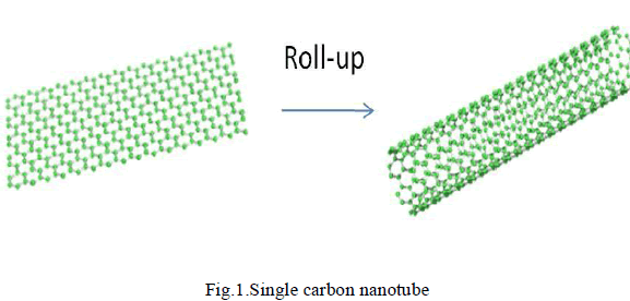
| A carbon nanotube field-effect transistor (CNTFET) refers to a field-effect transistor that utilizes a single carbon nanotube as shown in Fig 1. First demonstrated [1] in 1998, there have been major developments in CNTFETs. According to Moore's law, the dimensions of individual devices in an integrated circuit have been decreased by a factor of approximately two every two years. |
 |
| This scaling down of devices has been the driving force in technological advances since late 20th century. The limits involve electron tunneling through short channels and thin insulator films, the associated leakage currents, passive power dissipation, short channel effects, and variations in device structure and doping. These limits can be overcome to some extent and facilitate further scaling down of device dimensions by modifying the channel material in the traditional bulk MOSFET structure with a single carbon nanotube or an array of carbon nanotubes. |
LITERATURE SURVEY |
| Martel R et al (1998) fabricated field effect transistors based on individual single- and multi-wall carbon nanotubes and analysed their performance [1]. Transport through the nano tubes is dominated by holes and, at room temperature; it appears to be diffusive rather than ballistic. By varying the gate voltage, then he successfully modulated the conductance of a single-wall device by more than 5 orders of magnitude. Multi-wall nanotubes show typically no gate effect, but structural deformations in their case a collapsed tube can make them operate as field-effect transistors. These predictions have been verified in recent scanning tunnelling spectroscopy experiments. |
| In 2004, Nguyen TK et al formulated low-noise amplifier (LNA) design techniques applied to the cascade topology based on CMOS technology: classical noise matching, simultaneous noise and input matching (SNIM),powerconstrained noise optimization, and power-constrained simultaneous noise and input matching (PCSNIM) techniques [2].Based on the noise parameter equations, this paper provides clear understanding of the design principles, fundamental limitations, and advantages of the four reported LNA design techniques so that the designers can get the overall LNA design perspective. As a demonstration for the proposed design principle of the PCSNIM technique, a very low-power folded-cascade LNA is implemented based on 0.25- m CMOS technology for 900-MHz Zigbee applications. The overall behaviour of the implemented LNA shows good agreement with theoretical predictions. |
| Singh D.V (2005) introduced direct measurements of frequency response of CNFET [3]. Here the frequency response of CNFET biased in the common-source and common-gate configurations has been measured up to 200 MHz for the first time using a direct measurement technique. In this frequency range there is no observed degradation in the measured AC response of the CNFET. The effect of parasitic capacitance on the measurement has been identified and based on a simple model; it is estimated that this approach can be extended well into the Gigahertz range. This is the only demonstrated method of directly characterising the frequency response of nano scale devices where the signal levels are below the noise floor of conventional network analysers. |
| Lin YM et al (2006) presented low-frequency current fluctuations in Individual Semiconducting Single-Wall Carbon Nanotubes. It includes systematic study on low-frequency current fluctuations of nanodevices consisting of one single semiconducting nanotube, which exhibit significant 1/f-type noise [4]. By examining devices with different switching mechanisms, carrier types (electrons v/s holes), and channel lengths, he showed that the 1/f fluctuation level in semiconducting nanotubes is correlated to the total number of transport carriers present in the system. These results not only provide the basis to quantify the noise behaviour in a one-dimensional transport system but also suggest a valuable way to characterize low-dimensional nanostructures based on the 1/f fluctuation phenomenon. |
| In 2006, Zhang M et al gives Radio-frequency transmission properties of carbon nano tubes in a field-effect transistor configuration [5]. In this letter, the radio-frequency (RF) transmission properties of single-walled carbon nanotubes (CNTs) have been characterized up to the frequency of 12 GHz in a carbon nanotube field-effect transistor (CNFET) configuration using a two-port S-parameter method for the first time. The RF characteristics of the CNTs were measured from the drain to the source of the CNFET.A resistance, inductance, and capacitance model has been proposed, and the element values have been extracted. Without the effect of the parasitic, the RF signal transmission in the CNTs presents no degeneration even at 12 GHz. |
| Deng J et al (2007) introduced a compact spice model for carbon-nanotube field-effect transistors including nonidealities and its application [6]. The modelled non-idealities include the quantum confinement effects on both circumferential and axial directions, the acoustical/optical phonon scattering in the channel region, and the screening effect by the parallel CNTs for CNFET with multiple CNTs. In order to be compatible with both large and small-signal applications, a complete transcapacitance network is implemented to deliver the real-time dynamic response. He implemented this model with an HSPICE. The model described in this paper serves as a starting point toward the complete CNFET device model incorporating the additional device/circuit-level non-idealities and multiple CNTs. Comparison with a more accurate device model using the tight binding band-structure model shows that this model is valid for CNFET with a wide range of diameters. |
| Paul BC. (2007) introduces the Impact of a Process Variation on nanowire and nanotube Device Performance [7]. Although every process parameter variation drastically affects the conventional MOSFET performance, he found that nanowire/nanotube FETs are significantly less sensitive to many process parameter variations due to their inherent device structures and geometric properties. It is observed that a two-input NAND gate with nanowire or nanotube FETs shows a more than four times less performance variation than its bulk MOSFET counterpart and about two times less than FinFET devices at the 45 and 32 nm technologies, respectively. |
| In 2008,LiangtiQu gives an idea about high frequency noise in manufacturable carbon nanotube transistors[8]. In that time HF noise parameters were measured and modelled for the first time for wafer-scale manufacturable CNTFETs. These first multi-tube multi-finger CNTFETs exhibit still relatively high values for the minimum noise figure (NFmin = 3.5 dB at 1 GHz). Based on detailed compact modeling, the origin of this noise can be explained by the existence of the parasitic network and metallic tubes with high-frequency noise parameters. |
| Amlani (2009) presented frequency response function (FRF) showing ac gain from a single-walled carbon nanotube transistor [9]. A top-gated carbon nanotube FET (CNFET) is configured as a common-source amplifier and the FRF of the amplifier is measured. Evidence of unambiguous signal amplification is observed in time domain as well as frequency domain up to a unity voltage gain frequency of approximately 560 kHz. The observed roll-off in frequency is solely due to the RC time constant of the measurement apparatus. A specifically designed circuit-compatible SPICE model for the CNFET is used to model both dc and ac characteristic with the same set of physical parameters. |
| In 2011, Momeni et al introduced a systematic approach to designing high frequency and high power oscillators using activity condition [10] .This method finds the best topology to achieve frequencies close to the Fmax of the transistors. He also determines the maximum frequency of oscillation for a fixed circuit topology, considering the quality factor of the passive components. Using this technique, in a 0.13 m CMOS process, he designed and implemented 121 GHz and 104 GHz fundamental oscillators with the output power of 3.5 dBm and 2.7 dBm, respectively. Next, he introduced a novel triple-push structure to realize 256 GHz and 482 GHz oscillators. The 256 GHz oscillator was implemented in a 0.13 m CMOS process and the output power of 17 dBm was measured. The 482 GHz oscillator generates 7.9 dBm (0.16 mW) in a 65 nm CMOS process. This approach has applications in millimeter-wave frequencies for communication and radar systems as well as terahertz band for bio- and molecular spectroscopy and imaging. |
| In 2011, Koswatta et al introduces RF performance potential of carbon electronics[11]. Carbon electronics based on carbon nanotube array field-effect transistors (AFETs) and 2-D graphene field-effect transistors (GFETs) have recently attracted significant attention for potential RF applications. Here, he explores the ultimate RF performance potential for these two unique devices using semi classical ballistic transport simulations. It is shown that the intrinsic current-gain and power-gain cut off frequencies above 1 THz should be possible in both AFETs and GFETs. Thus, both devices could deliver higher cut off frequencies than traditional semiconductors such as Si and III–V’s. In the case of AFETs, he shows that their RF operation is not sensitive to the diameter variation of semiconducting tubes and the presence of metallic tubes in the channel. |
| Paydavosi N et al (2011) introduces a RF performance potential of array-based carbon-nanotube transistors [12]. A comprehensive study, which is presented in two parts, is performed to assess the radio-frequency (RF) performance potential of array-based carbon-nanotube field-effect transistors (CNFETs). The time-dependent boltzmann transport equation is solved self consistently with the poisson equation to study the impact of nanotube phonon scattering on different aspects of intrinsic (single-tube, contact-independent) CNFET operation, including the attainable drive current and transconductance per tube, the intrinsic cut off frequency, the intrinsic y-parameters, and the small-signal equivalent circuit for the intrinsic transistor. |
| Zhang J et al (2011) proposed Carbon Nanotube Variations through Co-optimized Technology and Circuit Design [13]. The main contributions are comprehensive analysis quantifies the impact of CNT-specific variations on the overall delay variations of CNFET digital VLSI circuits. For example, CNT variations candegrade potential speed benefits of CNFET circuits by 60% at the 16nm technology node. |
| Salamat S etal (2011) introduces an Intrinsic Performance Variability in Aligned Array CNFETs[14].The I–V characteristic of carbon nanotube (CNT)transistors is dictated by the Schottky barrier (SB) at metal–nanotube interface. Given the wide distribution of diameter of CVD-grown nanotubes, the presumption of single SB, however, is inappropriate for transistors with aligned array of CNTs. Indeed, array transistors with similar geometries and contact material can still exhibit considerable variation in threshold voltage (VT ), ON current (ION), and device resistance (Rd).The measured diameter distribution within the framework of detailed numerical simulations to demonstrate that the diameter distribution of CNTs (in CNT FETs) plays a dominant role in defining the fluctuation of array transistors. Besides, it is argued that the large scale integration of these devices within an IC would be feasible only if the distribution of diameter is considerably narrowed. |
| IannacconeG (2011) introduced the shot noise properties of carbon-based transistors in which the channel is laterally confined, either in the form of grapheme Nano ribbons or of carbon nanotubes[15]. The model and with computationally-intensive statistical simulations that electron-electron interaction can lead to a significant suppression of shot noise, often overlooked when the device is described with the Landauer-Buttiker formalism. Finally, inter band tunneling can play a significant role in enhancing shot noise due to exchange of holes between drain and channel, that is a peculiar effect observable in the case of channel materials with very small energy gaps. |
| Sakalas, P (2011) measured and modeled HF noise parameters for the first time for wafer-scale manufacturable CNTFETs 16]. Based on detailed compact modelling, the origin of this noise can be explained by the existence of the parasitic network and metallic tubes. In 2013, Schroter M etal introduces the Carbon Nanotube FET Technology for Radio-Frequency Electronics. The carbon-based electronics is an emerging field[17]. Its present progress is largely dominated by the materials science community due to the many still existing materials-related obstacles for realizing practically competitive transistors. Thispaper provides an overview on the state-of-the-art of CNTFET technology from an electrical engineering and radio frequencyanalog applications point of view. Important material properties, resulting device structures, their fabrication, and the most relevant modeling concepts are briefly reviewed. |
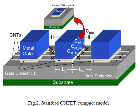
| In 2014, Landauer GM et al introduces a Radio-Frequency performance of carbon nanotube-based devices and circuits considering noise and process variation [18]. This paper provides a global overview of the radiofrequency (RF) performance potential of carbon-nanotube field effect transistors (CNFET), which for the first time includes theimpact of noise. The developed noise and manufacturing process variability extensions for the Stanford CNFET compact model, implementedin Verilog-A and compatible with conventional circuitsimulators. CNFET figures-of-merit (FoM) are determined bothon the device and on the circuit level. |
| The extended model is applied for a detailed simulation study on the CNFET technology’s RF behavior, both on device and circuit level. The assumed CNFET device can outperform MG Si- CMOS in most ITRS RF CMOS benchmark categories. For these device-level FoMs the CNFET technology has years of performance advantage over Si-CMOS, and good scalability shows promise for maintaining this advantage once having arrived at the market. One weak point is high flicker noise, which yet is inherent to highly scaled devices with a low number of charge carriers in the channel. It indicates the need for optimized manufacturing methods with low αH. |
 |
CONCLUSION |
| This paper presented Radio-Frequency performance of carbon nanotube-based devices and circuits. Emphasis is put on the description of suppressed channel shot noise. The development of these two extensions has been motivated by a lack of compact models for realistic RF simulations. The extended model is applied for a detailed simulation study on the CNFET technology’s RF behaviour, both on device and circuit level. For these device-level FoMs the CNFET technology has years of performance advantage over Si-CMOS, and good scalability shows promise for maintaining this advantage once having arrived at the market. One weak point is high flicker noise, which yet is inherent to highly scaled devices with a low number of charge carriers in the channel. It indicates the need for optimized manufacturing methods with low αH. For the first time, circuit-level FoMs for CNFET-based RF building blocks are presented. Simple CNFET-based LNA topologies are already competitive with the most advanced CMOS designs in terms of FoMLNA. CNFET oscillators clearly outperform their silicon counterparts regarding FoMVCO. By using CNFETs very high operating frequencies can easily be achieved. These promising results rely on a tube growth process with a well-behaving CNT diameter distribution, a sufficiently high CNT array density, and a diminishing percentage of mCNTs, while unoptimized growth processes result in performance penalties. In summary, the CNFET is predicted to outperform Si-CMOS in RF applications, a field which has become a main driving force for the semiconductors industry. This encourages the improvement of today’s CNFET manufacturing technologies up to market insertion, as carbon nanotubes may enable a future high-performance low-cost SoC scenario. |
References |
|