International Journal of Innovative Research in Science, Engineering and Technology
ISSN ONLINE(2319-8753)PRINT(2347-6710)
ISSN ONLINE(2319-8753)PRINT(2347-6710)
F.Y. Al- Shaikley1, M.F.A.Alias2, A.A.Alnajjar3, A.A.J.Al-Douri4
|
| Related article at Pubmed, Scholar Google |
Visit for more related articles at International Journal of Innovative Research in Science, Engineering and Technology
Thin films of undoped and doped CdTe with thickness around 500±10nm were deposited by thermal evaporation technique onto (100) p-GaAs wafer. The effect of both Al and Sb dopant percentages (0.5, 1.5 and 2.5) and substrate temperatures (RT and 423K) on the optoelectronic properties of CdTe/p-GaAs heterojunction was studied. IV characteristics under illumination for the prepared CdTe/p-GaAs heterojunctions showed a good significant photovoltaic effect. The value of short circuit current (Isc) for CdTe/p-GaAs heterojunction doped with Sb was higher than that doped with Al. The effect of Al doping on the value of the open-circuit voltage (Voc) was more than Sb doped. The outcomes of all these measurements for various (Al and Sb)doping of thin CdTe deposited on GaAs were indicated that 2.5%Sb-doped CdTe/p-GaAs heterojunctions deposited at RT and 423K posses a good response to illumination which make it a candidate for heterojunction device used as basic for fabricating photo sensors
Keywords |
| CdTe/p-GaAs heterojunction, Al and Sb dopant, I-V characterization. |
I. INTRODUCTION |
| The fabrication of II-VI/III-V heterojunctions has been a topic of great interest due to their potential applications in optoelectronic devices [1]. The most promising of these devices had cadmium telluride (CdTe) as one of the semiconductors in the junction. CdTe is a unique among II-IV group of binary semiconducting compounds, as it has both p- and n-type conduction [2]. This permits the fabrication of solar cells in both homo- and heterojunction configuration [3-6]. Its band gap about 1.5eV, just in the middle of the solar spectrum, and possess high absorption coefficient (α) (>104 cm–1) for the visible solar spectrum make CdTe very good candidate material for photovoltaic conversion [7]. Moreover CdTe has attracted much attention for producing X-ray and gamma-ray detectors operating at room temperature [8,9], as well as a buffer layer for the growth of Hg1-xCdxTe or Hg1-x(CdyZn1-y)xTe for infrared detectors [10-12] and it is a promising host material as doping with magnetic impurities such as Co, Fe, Mn for magneto-optic devices [13-15]. |
| The use of III-V semiconductors substrates such as GaAs has been largely explored in photonic and high-speed optoelectronic monolithic devices due to their direct band gap and the possibility to use them as high-quality massive substrates [16]. Thin CdTe films are usually grown on GaAs substrate, despite the high lattice mismatch between CdTe and GaAs, because the strain induced by lattice mismatch can be relaxed by misfit dislocations [17]. |
| Several techniques had been reported to the growth of CdTe on GaAs substrates, such as pulsed laser deposition (PLD) [18], hot wall epitaxy (HWE) [19], metal organic chemical vapor deposition (MOCVD) [20], radio frequency (RF) sputtering [21], molecular beam epitaxy (MBE) [22], and thermal evaporation method [23].. |
| The main focus of this work is to study the optoelectronic properties of CdTe/p-GaAs heterojunctions fabricated using thermal evaporation technique. This method is much less complicated than the techniques currently used for fabrication CdTe / GaAs heterojunction. The effect of dopant concentration of Al and Sb at both substrate temperatures (RT and 423K) on the optoelectronic properties for CdTe/p-GaAs heterojunctions has been investigated. |
II. EXPERIMENTAL PROCEDURE |
| Heterojunctions of CdTe/GaAs have been fabricated at both substrate temperatures (Ts) equal to room temperature (RT) and 423K by thermal evaporation technique at vacuum about 10-6 Torr using the Edward E306A coating system. The thickness (t) of undoped and doped CdTe with various weight percentages (0.5, 1.5, and 2.5) of Al and Sb was around 500±10nm. The p-type of GaAs wafer (Zn-doped GaAs (p=(1-5)x1017cm–3)) with thickness 600μm and (100) orientation was used in this work. A GaAs wafer was clean and prepare with processes mentioned in ref. [24]. |
| The illuminated current-voltage (I-V) characteristics at room temperature under forward and reverse bias voltages within the range and (–2.0-2.0)V for CdTe/GaAs heterojunction prepared with various deposition conditions were performed with different intensities (20, 60 and 100)mW/cm2 measured by solar meter by using a Halogen lamp type Kaiser at Sharjah University, Sharjah-UAE. |
III. RESULTS AND DISCUSSION |
| The current-voltage characteristics under illumination are one of the optoelectronic characteristic for heterojunction. The photocurrent is considered as an important parameter that plays an effective role in solar cell devices. |
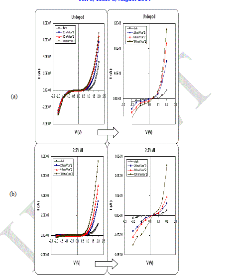
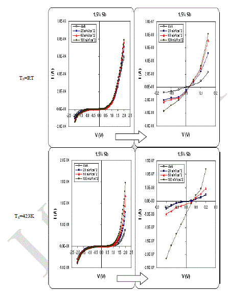
| The I-V characteristics at the forward and reverse-bias voltage in dark and under illumination from the CdTe side, with various light intensity (20, 60 and 100 mW/cm2) for undoped and doped CdTe/p-GaAs heterojunctions with various doping percentage of Al and Sb deposited at RT and 423K are investigated. From this investigation, it has been selected some of heterojunctions which are possessed more sensitivity to illumination than the other prepared heterojunctions. The current-voltage characteristics under illumination of the selected heterojunctions are shown in Figs.1,2,3 for CdTe/p-GaAs. It is observed that, in general, the forward I-V characteristics in dark of these heterojunctions show the exponential rise at low voltage (below 0.2V). This is due to the decrease in the width of depletion region at the junction as a result of an increase in the majority carriers injected by the applied voltage which lead to the decrease in the built-in potential. As the bias is increased the forward current (If) increases and the deviation from the exponential behavior is highlighted in these figures. At higher voltage the I-V dependence are linear due to the influence of appreciable series resistance on the junction characteristics [24]. Upon illumination of the junction, more carriers are generated and forward current increases. |
| Figs.1,2,3 show the I-V characteristics for undoped and 2.5% Al-doped CdTe/p-GaAs heterojunctions deposited at 423K and for 1.5% and 2.5% Sb-doped heterojunctions deposited at RT and 423K respectively. It is seen that the illuminated forward current increases with increasing the incident light intensity and with increasing the bias voltage. |
 |
 |
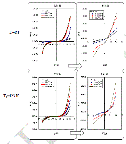 |
| Also it is clear that illuminating the junctions increased the reverse bias current as expected from the electron-hole pair generation in the depletion region if the incident photon energy is greater than the smallest direct band gap of the heterojunction [25]. |
| The generated electron-hole pairs within the depletion width, and within a diffusion length outside of the depletion width are quickly swept away due to the strong electric field producing the photocurrent in the reverse-bias direction which increases with increasing of the incident light intensity due to the increase in the number of photo generated electrons and holes in the depletion region [25]. |
| Another noticeable remark from Figs.1,2,3 is that, in general, the effect of illumination on the reverse current (Ir) for heterojunction doped with 2.5%Al deposited 423K is more than those for doped with 2.5%Sb and undoped heterojunctons. Also it is found that Ir increases about one order of magnitude with increasing of the incident light intensity to 100mW/cm2 at reverse bias voltage equal to 0.2V. |
| The results of the current-voltage characteristics under illumination for CdTe/n-GaAs heterojunctions in earlier paper [23] showed more significant photovoltaic effect than for CdTe/p-GaAs heterojunctions in the present work. The outcome of above measurements indicates clearly a good response of these prepared heterojunctions to illumination which makes them a candidate for fabrication optoelectronic devices. This required a lot of investigation to enhance this response by look for other parameters such as thickness of film, annealing temperature and also to study the surface analysis of heterojunction with conjunction with various parameters.The short circuit current (Isc) and open circuit voltage (Voc) are among several main parameters used to describe device behavior and quality. |
| Figs.4 (a and b) illustrate the variation of Isc and Voc as a function of doping percentage of Al and Sb in the CdTe thin film for CdTe/p-GaAs heterojunctions, which deposited at RT and 423K and illuminated at a light intensity of 100mW/cm2 (AM1). Fig.4 (a) shows that the increasing in doping percentage caused an increase in the value of Isc about one order of magnitude for Al-doped CdTe/p-GaAs heterojunctions deposited at RT and 423K, however opposite trend has been observed for heterojunction deposited at RT and doped with 2.5%Al, i.e., the value of Isc is decreased. The increase in doping percentage of Sb from 0.5% up to 2.5% resulted to an increase in Isc around a factor of five times and one order of magnitude for heterojunctions deposited at RT and 423K respectively. In general, it can be noticed that the effect of both Ts on Isc for heterjunction doped with Sb is clearer than for heterojunction doped with Al. The value of Isc for Sb-doped heterojunction is more than that for heterojunction doped with Al. |
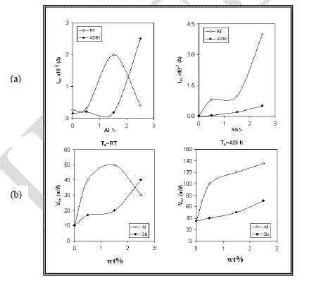 |
| In general, Fig.4 (b) illustrates that the effect of Al doping on Voc is more than that for doped with Sb at both deposition temperatures. The value of Voc is increased around a factor of five and four for Al- and Sb-doped heterojunctions deposited at RT with increasing doping to 1.5% and 2.5% respectively. An opposite trend is shown for heterojunction doped with 2.5 %Al and deposited at RT.On the other hand, the value of Voc is increased about one order of magnitude and around a factor of two times for heterojunctions doped with Al and Sb which deposited at 423K respectively. Another noticeable remark is that the value of Voc for heterojunctions deposited at 423K is more than that deposited at RT for both types of doping. |
| The reduction in the Isc and Voc values can be attributed to various factors such as the presence of series resistance, doping concentration on both sides of the junction, and high defect density as a result of the large lattice mismatch between CdTe and GaAs which give rise to allowed energy states within the band gap and i.e within the depletion region and these interface states introduce very effective recombination centres for the photo generated electrons and holes [26, 27]. |
IV. CONCLUSION |
| Studies of I-V characteristics under illumination with various light intensity ( 20, 60 and 100) mW/cm2 for CdTe/p- GaAs heterojunctions were performed in an attempt to enhance understanding how processing steps including the addition of aluminium, antimony in CdTe thin film and substrate temperature affects the heterojunction's properties. From the results of these studies it can conclude that: |
| I-V characteristics under illumination for CdTe/p-GaAs heterojunctions showed a good significant photovoltaic effect. |
| In general, the value of Isc for CdTe/p-GaAs heterojunction doped with Sb is more than that for Al-doped. |
| The effect of Ts on Isc for heterjunction doped with Sb is more clear than for heterojunction doped with Al |
| The influence of Al doping on Voc is higher than that for Sb at both Ts. |
| The value of Voc for heterojunctions deposited at 423K is more than that deposited at RT for both types of doping. |
| CdTe/p-GaAs heterojunctions doped with 2.5%Sb in CdTe thin films deposited at RT and 423K indicate clearly a good response to illumination which make it a candidate material for fabricating optoelectronic devices. |
References |
|