Keywords
|
| Adiabatic technique, Dynamic power dissipation, Asymmetrical,Comparator |
INTRODUCTION
|
| Power dissipation reduction is an important issue which need to be focussed for latest demand of technology. As in conventional cmos power dissipation is evaluated by two factors:1) static power dissipation 2) dynamic power dissipation. Dynamic power dissipation occurs in charging and discharging of capacitive loads. During charging, current flows from Vdd to capacitive loads while in discharging, current flows from capacitive load to ground.8Total charge transferred during charging/discharging cycle: Q = CL Vdd .Thus, an energy of E= CLVdd 2 is drawn from the power supply during charging. By assuming that the energy taken equals the energy supplied to the load capacitor, the energy stored into the load CL is half of the supplied energy: Estored = ( 1/2 )CL Vdd 2. The other half is dissipated in R. The same amount of energy is dissipated during the discharge process . Therefore the total dissipation as heat during charging and discharging is |
| Echarge = Edischarge =1/2CL Vdd 2 |
| Adiabatic technique is used to incease energy efficiency of logic circuit in thermodynamic. For energy recovery circuit, the ideal energy dissipation when a capacitance C is charged from 0 to Vdd or discharged from Vdd, through a circuit of resistance R during time T is given by E= (RC/T) Vdd 2 When T >> RC, the power consumption is much smaller. Q is the charge transferred to the load, C is the value of the load capacitance, R is the on-resistance of the PMOS switch, V is the final value of the voltage at the load, T is the charging time. |
| Adiabatic charging may be achieved by charging the capacitor from a time varying source that starts at Vi= 0V. This requires sinusoidal power supply. Theoretically, it is possible to reduce the power dissipation by extending the switching time. In this paper we are introducing ultra low power comparator which is designed with differrent adiabatic technique. Proposed comparator using the two phase split level power supply to reduce the power dissipation. As arithmetic circuits are the basic building blocks of many of the digital circuits, the present paper mainly concern on its design. |
POSITIVE FEEDBACK ADIABATIC LOGIC
|
| PFAL is new adaibatic technique which utilizes positive feedback1. This logic structure consist of cross-coupled inverters, with NMOS devices are connected between the outputs and the power-clock. In PFAL, sinusoidal power supply is used, known as power clock which is divided into four phases.3 In evaluate interval , the outputs are evaluated from stable input signal. During hold interval, output are kept stable , next is the recover interval, which recover the energy and the last is wait interval , inserted for the symmetry. PFAL is a dual-rail circuit which accept complementary inputs with respect to each other and provide outputs complemented with each other with partial energy recovery. The general schematic of the PFAL gate is shown in Fig1. consist of an adiabatic amplifier, a latch made by the two PMOS and two NMOS , output nodes out and outB without any degradation in logic level . The functional blocks are in parallel with the PMOSFETs of the adiabatic amplifier and form a transmission gate. The two n-trees realize the logic functions. |
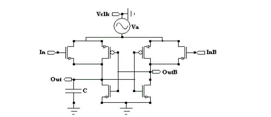
Fig1. PFAL logic circuit |
TWO PHASE ADIABATIC STATIC CLOCKED LOGIC
|
| The Two Phase Adiabatic Static Clocked Logic (2PASCL) uses two phase clocking split level sinusoidal power supply’s which has symmetrical and asymmetrical power clocks where one clock is in phase while the other is out of phase.7 The circuit has two diodes in its construction where one diode is placed between the output node and power clock, and another diode connected between one of the terminals of NMOS and power source. Both the MOSFET diodes are used to recycle charges from the output node and to improve the discharging speed of internal signal nodes. The circuit operation is divided into two phases “hold phase” and “evaluation phase”. During the evaluation phase, the power clock swings up and power source swings down. During the hold phase, the power source swings up and power clock swings down. |
 |
| Fig2. 2PASCL logic circuit |
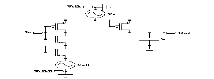
PROPOSED ADIABATIC LOGIC
|
| Proposed adiabatic logic is a combination of both PFAL and 2PASCL. Its structure is similar to 2PASCL except the core part of 2PASCL is replaced by PFAL logic circuit and uses two phase split level sinusoidal power supplies which is denoted by Va and VaB. The circuit operates in two phases, evaluation and hold, in evaluation phase, Va swings up and VaB swings down, and in hold phase, VaB swings up and Va swings down. Let us assume, during evaluation phase the input (In) is high and input (InB) goes low accordingly, consequently M3 is conducting and output (OutB) follows the power supply Va, and at the same time M1 gets turned ON by output (Out ) and thus reduces the charging resistance. Being in parallel with M3 and during hold phase, charge stored on the load capacitance CL flows back to power supply through M1. So that power dissipation is reduced. The proposed circuit uses two MOS diodes, one is connected to Out and Va and other diode is connected between common source of M5- M6 and other power supply VaB, Both the MOS diodes are used to increase the discharging rate of internal nodes. |
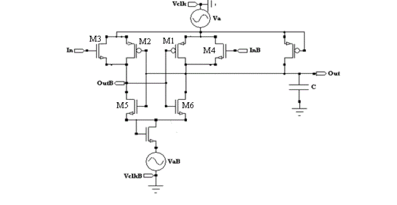
Fig3. Proposed adiabatic logic circuit |
DESIGN AND SIMULATION
|
| A.CMOS COMPARATOR |
| Conventional cmos comparator consist of Pmos pull up network and Nmos pull down network having two inputs IN1 & IN2 and three outputs as shown in figure. This circuit uses dc supply. The total charge/discharge cycle has required an energy CVdd 2 half being dissipated in charging and half being used for information storage before it too is dissipated during discharge.Logic circuit and simulated waveform of conventional cmos comparator shown in fig 4. & fig 5. |
 |
| Fig 4. Conventional cmos comparator circuit |
 |
| Fig5.Simulated waveform conventional cmos comparator |
| B. PFAL COMPARATOR |
| A single bit adiabatic PFAL comparator is designed in S Edit is given in figure 6 .The core of PFAL logic is a latch made up of two PMOS and two NMOS transistors that avoid logic level degradation on the output nodes. The logic function in the functional block can be realized with only NMOS transistors connected parallel to the PMOS transistors. Its advantage as implementing both the true function and its complimentary function. Comparator having two input and determines whether one number is greater than, less than or equal to the other number. From the bottom, the graph shows the input signals IN1 and IN2 which are CMOS- compatible rectangular pulses. The third and fourth graph shows the output waveform of a correctly functioning single bit comparator, three outputs in which first is the IN1 is greater IN2, next is the IN1 is equal to IN2 and the last IN2 is greater than the IN1 which are simulated in spice The next graph demonstrates the voltage driver supply clock which is simulated using SPICE. Simulated waveforms shown in figure 7.c |
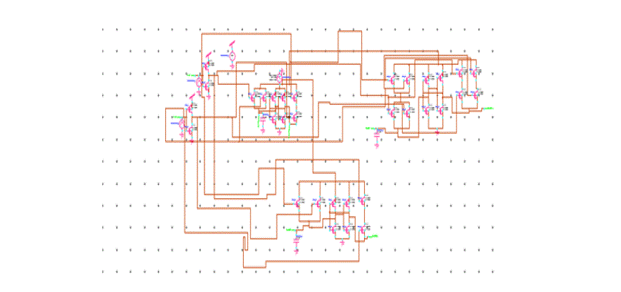
Fig6. PFAL comparator circuit |
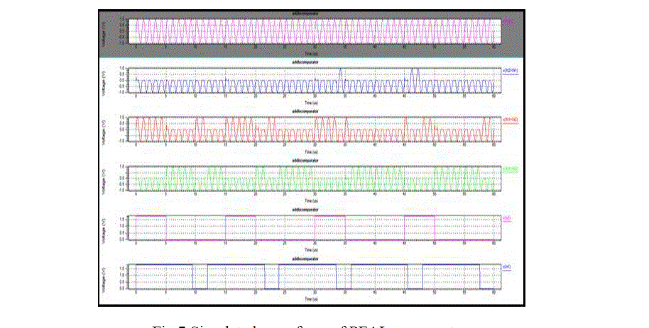
Fig 7.Simulated waveform of PFAL comparator |
| C. PROPOSED SINGLE BIT COMPARATOR |
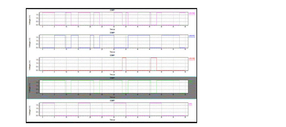
| Proposed Comparator circuit is combination of pfal and 2 pascl logic structure is shown in fig8. and simulated waveform is shown in fig9. It uses two phase split level sinusoidal power supply. The circuit operation is divided into two phases “hold phase” and “evaluation phase”. During the evaluation phase, the power clock swings up and power source swings down. During the hold phase, the power source swings up and power clock swings down. . Both the MOSFET diodes are used to recycle charges from the output node and to improve the discharging speed of internal signal nodes. From the bottom, the graph shows the input signals IN1 and IN2 which are CMOS- compatible rectangular pulses. The third and fourth graph shows the output waveform of a correctly functioning single bit comparator, three outputs in which first is the IN1 is greater IN2, next is the IN1 is equal to IN2 and the last IN2 is greater than the IN1 which are simulated in spice The next two graphs demonstrates the voltage driver supply clock which is simulated using SPICE. |
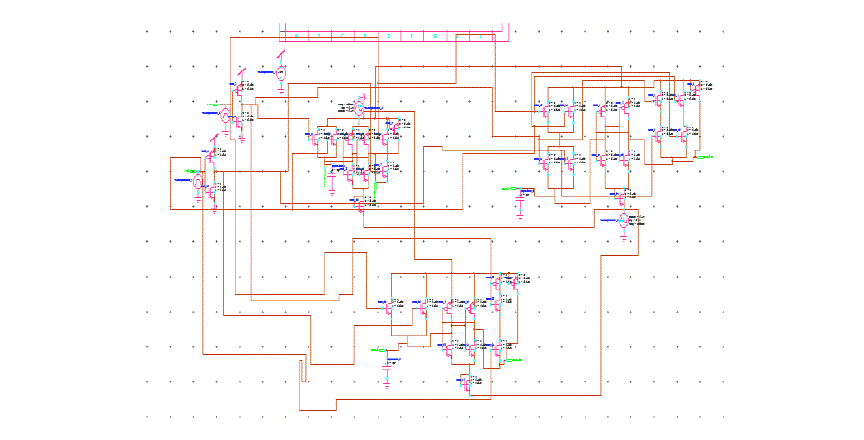
Fig 8. Proposed comparator circuit |
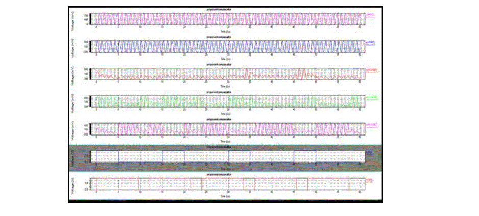
Fig 9.Simulated waveform of Proposed Comparator |
SIMULATION RESULT
|
| In this paper we designed the single bit comparator using cmos, PFAL and proposed adiabatic technique and simulation has been done using SPICE simulation with 180nm, 1.8 V standard CMOS process. The W/L of nMOS and pMOS logic gates used is 2.5u & 250nm. A capacitive load CL is placed at output node . On the basis of average power consumption and transistor count, cmos comparator and proposed ultra low power comparator has been compared at different frequencies.The result of comparison is shown in the table . The comparison of the proposed circuit with other traditional methodologies has proved that power consumption with the proposed logic is far less as compared to CMOS and other adiabatic style.Table 1. Shows the average power consumption of proposed comparator at different frequencies which is in nw very less as compare to convention cmos which is in uw. Table 1 also shows the number of transistors used for these two circuits. |

Table1. Comparison of comparator in adiabatic logic with CMOS |
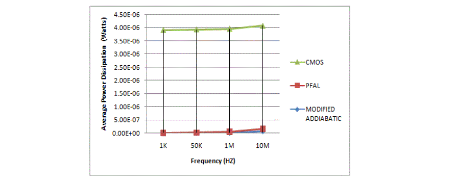
Figure 10 Average Power Dissipation Comparison between CMOS ,PFAL and proposed adiabatic logic |
CONCLUSION
|
| In this paper Depending on the application and the system requirements, this approach can be used to reduce the power dissipation of the digital systems but increase transistor count. Circuit simulations show that with the help of adiabatic logic, the energy savings of upto 98 % can be reached. I also analysed logic structure using modified adiabatic logic style which further reduces the power dissipation. I conclude that the adiabatic PFAL logic style and Modified Adiabatic logic style are advantageous in applications where power reduction is of prime importance as in high performance battery-portable digital systems running on batteries such as note-book computers, cellular phones and personal digital assistants. |
References
|
- Antonio Blotti and Roberto Saletti “Ultralow-Power Adiabatic Circuit Semi-Custom Design”Ieee Transactions On Very Large Scale Integration(Vlsi) Systems, Vol. 12, No. 11, NOVEMBER 2004
- A.K Maurya and Gagnesh Kumar “Energy Efficient Adiabatic Logic for Low Power VLSI Applications” International Conference onCommunication Systems and Network Technologies.,pp 460-464,2011.
- TanujaJaggi, Ravinder Kumar, Nidhi Sharma “ Power Efficient Positive Feedback Adiabatic Logic”,National Conference On Signal ProcessingAnd Communication Technology, May 2013.
- M. Pedram, “Power minimization in IC design: principles of applications,” ACM Transactions on Design automation of Electronic System, 1(1)pp 53-56, January 1996.
- Vetuli, S. Di Pascoli, and L.M. Reyneri, “Positive feedback in adiabatic logic, Electron.Lett”vol.32,pp1867- 1869 September 1996.
- Sung-Mo Kang And Yusuf Leblebici, CMOS Digital integerated circuits-Analysis and design, Mcgraw Hills,
- S. Samanta “Adiabatic Computing: A Contemporary Review,” International conference on computers and devices for communication, pp. 1-4,December 2009.
- N. Weste and K. Eshraghian, Principle of CMOS VLSI Design: A System Prospective, 2nd ed. New York: Addison – Wesley, 1993.
- G. Rama Tulasi and K. Venugopal “Design & Analysis of full adders using adiabatic logic” International Journal of Engineering Research &Technology (IJERT) ,VOL-I, July 2012.
|