International Journal of Innovative Research in Science, Engineering and Technology
ISSN ONLINE(2319-8753)PRINT(2347-6710)
ISSN ONLINE(2319-8753)PRINT(2347-6710)
Phani kumar TVB1, Nagraju N2, Santhosh Kumar Ch3
|
| Related article at Pubmed, Scholar Google |
Visit for more related articles at International Journal of Innovative Research in Science, Engineering and Technology
The microwave filter is a component which provides frequency selectivity in mobile, radar, satellite communication systems operating at microwave frequency. Microwave low pass filter suppress unwanted harmonic components above cut off frequency. Because of the distributed circuit elemental nature of the lumped components at microwave frequency, distributed lines like microstrip, striplines etc. are used as microwave low pass filter components. For stepped impedance filter design high and low impedance lines are used. This paper describes designing of Butterworth approximated stepped impedance low pass filter at 1.2 GHz with microstrip line implementation. Designed filter is simulated using Advanced Design System (ADS) software and is fabricated with photolithographic technique. The designed microwave component is tested with Rhode & Schwartz Network Analyzer and practical results are agreed with simulated one.
Keywords |
| Butterworth approximation, Stepped impedance, Richard’s transforms and Kuroda’s identities |
I. INTRODUCTION |
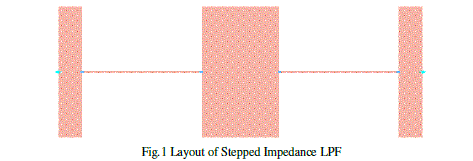
| Microwave filter is a two port, reciprocal, passive, linear device which attenuates heavily the unwanted signal frequencies while permitting transmission of wanted frequency. In general, the electrical performance of the filter is described in terms of insertion loss, return loss, frequency selectivity (or attenuation at rejection band), group delay variation in the pass band and so on. Filters are required to have small insertion loss, large return loss for good impedance matching with interconnecting components and high frequency selectivity to prevent interference. If the filter has frequency selectivity, and guard band between channels can be determined to be small which indicates that the frequency can be used efficiently. Also, small group delay and amplitude variation of the filter in the pass band are required for minimum signal degradation. Layout of Stepped impedance Low Pass Filter using Advance Design System Simulator is shown in Fig 1. |
| There are two methods of filter design. One is image parameter method and second is insertion loss method. The image parameter theory filter is based on the properties of transmission lines. A simple network with lumped components is described in terms of this continuous structure. In insertion loss method, a filter response is defined by a transfer function which is ratio of output voltage to the input voltage of the filter. The ideal low pass transfer function is characterized by a magnitude function that is constant in pass band and zero in stop band. Since such a low pass network can be represented by a quotient of finite degree rational polynomials, it is necessary to approximate it. The four classical solutions to the approximation problems are the Butterworth (maximally flat), Chebyshev (equal ripples in pass band), inverse Chebyshev (equal ripples in stop band) and elliptical (equal ripples in stop and pass band). Today most microwave filter designs are done with insertion loss method. |
 |
| The practical filters have small non-zero attenuation in the pass band and a small signal output in the stop band due to presence of resistive loss in reactive elements of propagating medium. The proposed microstrip stepped impedance low pass filter is designed for 1.2 GHz operating frequency with attenuation above 20 dB at 2.4 GHz in stop band. The stepped impedance distribution element filter is one of the most popular microstrip filter configuration used in lower microwave frequencies because of easy design, manufacturing and open circuited stub ends. |
| For this filter design microstrip line is a good transmission line due to advantages of low cost, compact size, light weight, planar structure and easy integration with other components on a single circuit board. Conventional filter structures like equal ripple and Butterworth low pass filter are requirements of special fabrication methods. Conventional low frequency techniques for fabrication does not fit at these frequencies due to the very high losses associated. Even though recent advent of novel materials and fabrication techniques like MMIC, MEMS, HTS and LTCC are available, thin microstrip film fabrication technique is preferred because of easiness. |
II. FILTER DESIGN |
| Above 900 MHz frequency, distributed nature of limped elements prevents the proper operation of filters. This paper presents for given specification, low pass filter is designed to achieve an exact center frequency, good bandwidth and low return loss level. Two major problems associated in microwave filter design are, first is within the limited frequency range only lumped elements work properly and second is distance between components at microwave frequency is not negligible. First problem is solved by Richard’s transforms which converts lumped elements into transmission line section. For second problem Kuroda’s identities can be used to separate filter elements by using transmission elements [2]. |
| Filters implementation using Richard’s transformer and kuroda’s identities have different lengths and widths of microstrip lines. However, to implement with alternative section of low and high characteristic impedance lines for LPF design stepped impedance technique is used. These filters are limited to the applications where sharp cut off frequency is not required. |
| A. LPF Design Procedure |
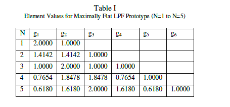
| For proposed design work we assume Butterworth approximation which gives maximum flat response in pass band. For normalized LPF design with source impedance 1 Ω and cut of frequency c ï· =1, the elemental values for ladder type circuits are tabulated in table 1 for N=1 to N=5. Figure 2 shows attenuation characteristics for various N versus normalized frequency. |
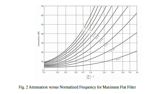 |
| In practical filter design procedure, it is necessary to determine the order of the filter. In this article, to design filter with more than 20 dB attenuation at 2.4 GHz, the order is selected from figure 2. Therefore (ω/ωc)-1=(2.4/1.2)-1=0.6, N=5 and filter element co efficient are g1=0.6180=C1, g2=1.6180=L2, g3=2=C3, g4=1.6180=L4, g5=0.6180= C5. Since the expressions for the inductor and capacitor of a filter depends on the characteristic impedance and length of microstrip line in stepped impedance filter design, high impedance line is chosen such that its narrow is not too much difficult to fabricate and low impedance line width must not allow any transverse resonance at operating frequency. |
| B. LPF is designed with fallowing specifications |
| Cut off frequency= 1.2GHz; characteristic impedance=50 Ω; High impedance=150 Ω; low impedance=10 Ω; dielectric constant= 2.55; In stepped impedance technique, the electrical lengths of inductor and capacitor sections are calculated from fallowing formulas [4] |
| βl=LRo/Zh(for inductors), βl=CZl/Ro( for capacitors)………(1) |
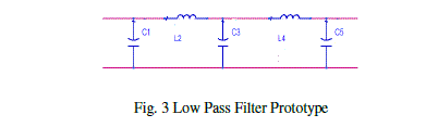
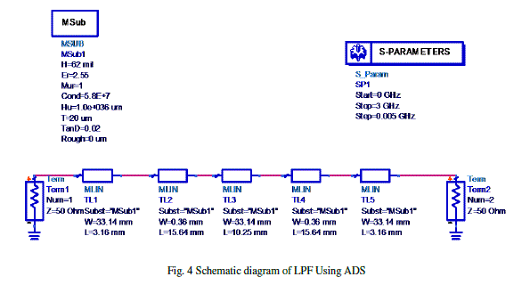
| The final filter prototype section is shown in Fig 3. The schematic diagram of LPF using Advance design system (ADS) software and photographic is show in Fig 4 and Fig 5 respectively. |
 |
III. RESULTS AND DISCUSSIONS |
| Calculated electric lengths of inductor and capacitors are βl1=g1Zl/Ro=7.080,βl2=g2R0/Zh=30.910,βl3=g3Zl/Ro=22.920, βl4=g4R0/Zh=30.910, βl5=g5Zl/Ro=7.080. The prototype low pass filter with center frequency of 1.2 GHz is fabricated with substrate of dielectric constant 2.55 and thickness of 62mil. The dimensions of the filter are calculated using line calculator tool in advanced design system (ADS) software. L1=3.16 mm, L2=15.64 mm, L3=10.25 mm, L4=15.24 mm, |
| L5=3.16 mm, W1=W3=W5=33.14 mm, W2=W4=0.36 mm. The prototype filter is tested with Rohde & Schwarz network analyzer. A comparison of simulated and measured frequency response is shown in Fig 6. |
 |
| The measured results are in good agreement with simulated results. Slight deviations are attributing to fabrication error and minimum insertion loss due to tow SMA connectors. The measured -3.0dB level is at 1.160 GHz and attenuation is about 27.544 dB at 2.4 GHz in simulation and from measurements -3.0dB level is at 1.2 GHz.. Up to 1 GHz frequency S11 parameter is below -10 dB, and hence it passes all frequency components without attenuation with in this frequency range (0-1GHz). Below table summarizes the complete filter dimension information. |
 |
IV. CONCLUSIONS |
| This article presents design of stepped impedance low pass filter with cut off frequency of 1.2 GHz and more than 20 dB attenuation in stop band. The design procedure is simple and it can be easily and inexpensively fabricated using common printed circuit board technology. It has high isolation and in a compact size. Moreover, any microwave low pass filter with good sharp cut off frequency and frequency selectivity can be designed using this structure. |
ACKNOWLEDGEMENTS |
| The authors would like to thank Pavan Kumar V for providing testing and development facility for this work and special thanks to Principal, HOD of ECE, Institute of Aeronautical Engineering College, Dundigal for support and encouragement. |
References |
|