


 15 / 22

Page 65
conferenceseries
.com
Volume 6
Research & Reviews: Journal of Material Sciences
ISSN: 2321-6212
Magnetic Materials 2018
October 22-23, 2018
October 22-23, 2018 | Rome, Italy
3
rd
International Conference on
Magnetism and Magnetic Materials
Nanoisland magnetic films: Technology and possible applications
Fedor Pudonin, Anatolii Boltaev, Dmitry Egorov
and
Igor Sherstnev
P.N. Lebedev Physical Institute of RAS, Russia
N
ow there has been a significant interest in the technology of obtaining and studying magnetic nanoisland films. This is
due both to the enormous applied potential of these objects. We used the RF-sputtering method to obtain nanoisland
films of magnetic materials such as FeNi, Co, Ni, etc. In this report we will present the results of our work on obtaining
magnetic nanoisland films and some applied aspects of these structures. Since the deposition rate is a stable value at constant
technological parameters, we deposit thin films whose effective thickness was determined by the time of deposition. There is
a critical thickness d*(percolation threshold) below which the films are nanoisland, and films with effective thickness d>d*
become continuous. To determine the d* value, we have grown several series of FeNi films with effective thicknesses from 0.5 to
3.0 nm with thickness steps Δ~0.07 nm. The standard polished ceramic plates (sitall), crystalline silicon, silicon nitride, glass,
as well as thin Al
2
O
3
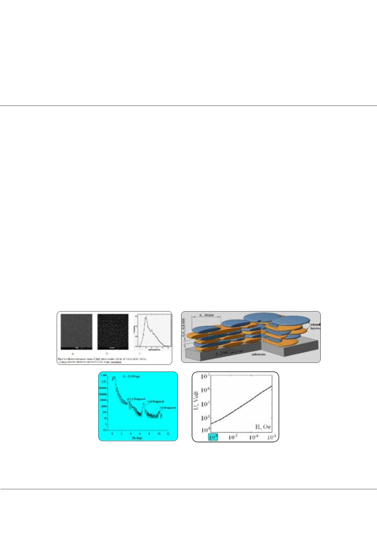
layers deposited on silicon were used as substrates. Figure 1 shows an image of some island FeNi films.
To determine d*, the dependences of the permittivity
ε
(
ω
) and conductivity
σ
on the thickness were studied. It was found
that Re
ε
(
ω
) and δ=[σ (T=300 K) - σ(T=77 K) simultaneously change sign at d~1.6-1.8 nm, which indicates the presence of
a percolation transition at d*~1.6-1.8 nm. Thus, FeNi films with an effective thickness d<1.6 nm are island. We have shown
that photoconductivity in the range 500-1500 nm, anomalous conductivity in weak electric fields, giant dielectric constant,
and other unusual properties are observed in nanoisland films of FeNi and other metals. We proposed to use nanoisland FeNi
films in which the effect of anomalous conductivity is observed as labels that can serve as a protection for various documents
and securities and other products. Nanoisland films can also be used to create sensors of superweak magnetic fields at room
temperature. For this, we fabricated multilayer island structures such as [FeNi/Co]
N
in figure 2. With the help of X-ray studies
it was shown that in such systems the island layers do not mix and they really are periodic structures. It was found that these
structures are capable of detecting (changing their resistance) magnetic fields H<10
-11
T. This is a great result and we hope to
improve it.
Figure 2:
Multilayer structure (FeNi-Co)N
Figure 3:
Angular dependence of the X-ray reflection I from the multilayer island structure [ZnTe(1.5 nm)–Ti(0.9) nm]10.
Figure 4:
The dependence of the voltage U on the structure (FeNi-Co)20 on the magnetic field H.
Fedor Pudonin et al., Res. Rev. J Mat. Sci. 2018, Volume 6
DOI: 10.4172/2321-6212-C6-029