


 13 / 22

Page 51
conferenceseries
.com
Volume 6
Research & Reviews: Journal of Material Sciences
ISSN: 2321-6212
Materials Physics 2018
August 16-17, 2018
August 16-17, 2018 | London, UK
4
th
International Conference on
Condensed Matter and Materials Physics
Interconnection of charge neutrality level with electronic structure and p-d hybridization and its
modification upon electronic excitation
Arkaprava Das
1
, Subodh K Gautam
1
, D K Shukla
2
, G R Umapathy
1
, S Ojha
1
and
Fouran Singh
1
1
Inter University Accelerator Centre, India
2
UGC-DAE Consortium for Scientific Research, India
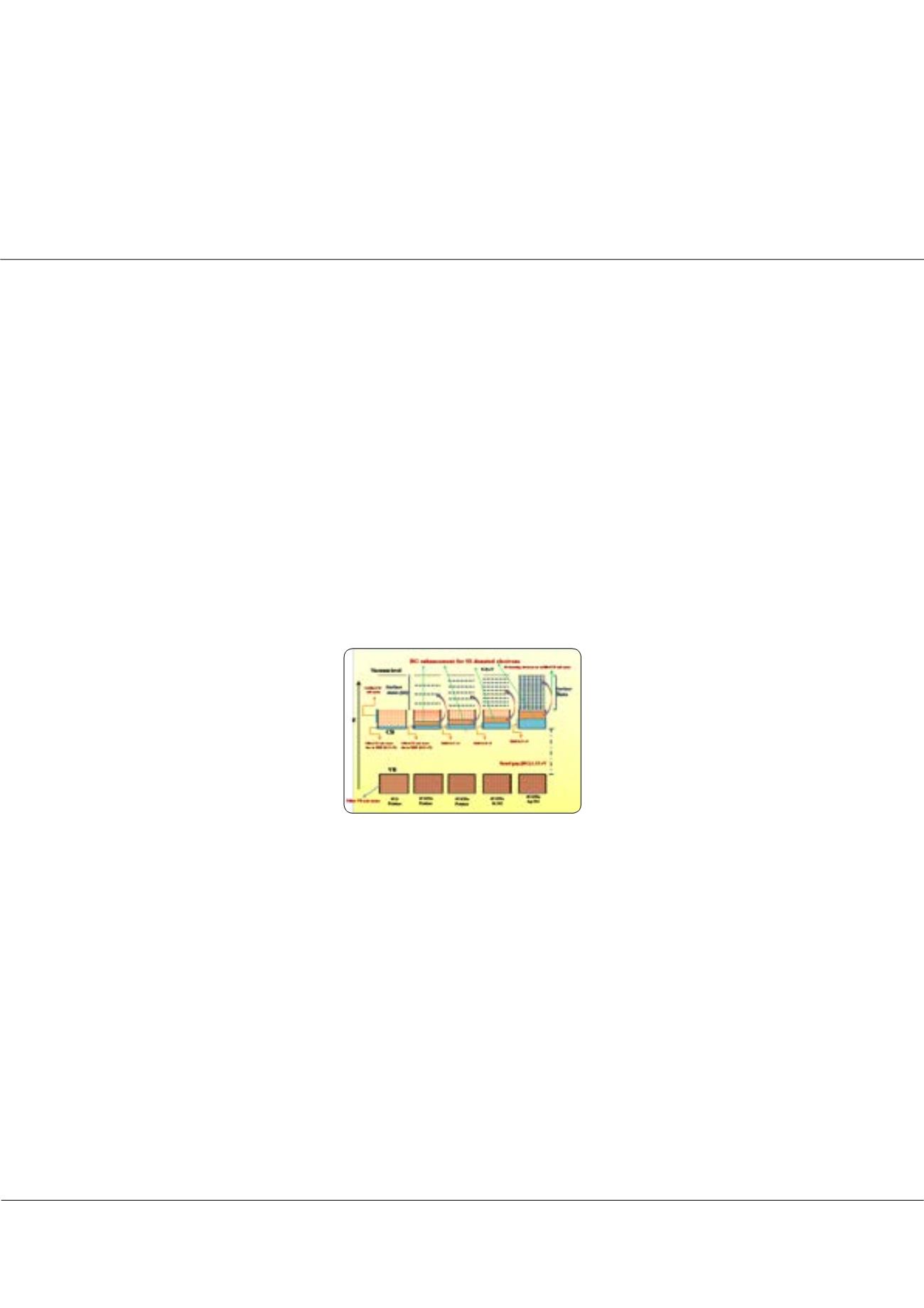
U
ndoped and tin doped cadmium oxide (CdO) based thin films are irradiated by 84 MeV Si
6+
and 120 MeV Ag
9+
ions. In
the present work the charge nutrality level (CNL) in highly conducting CdO thin films is demonstarted by the observed
variation in the band gap upon annealing and doping. The increase in crystallite size with tin doping is a signature of decrease
of CdO stoichiometry by substitutional replacement of Cd with Sn. Each Cd
2+
ions are substituted by Sn
2+
ions with reduction
of Sn
4+
via creating oxygen vacancies in the lattice which also enhnaces the carrier concentration in the tin doped thin film. The
band gap enhancement cannot be explained by Burstein Moss Shift (BMS) only but can be explained by formation of charge
neutrality level (CNL). The level of local CNL resides at the branch point of virtual gap states (ViGS) generation of which is the
consequence of tin doping in CdO lattice. Further investigations using soft X-ray absorption spectroscopy (SXAS) at oxygen
K and cadmiumM edge and the analysis of the spectral features has revealed an evidence of p-d interaction between O 2p and
Cd 4d orbitals. After irradiation, the thin films exhibit an unusual band gap enhancement via generation of oxygen vacancies
due to huge electronic energy deposition inside the lattice by Ag and Si ions. The observed band gap enhancement has been
substantiated by a schematic block diagram.
Recent Publications
1. Arkaprava Das et al. (2017) Virtual gap states induced modifications in charge neutrality level in cadmium oxide thin
films. Materials Research Express. 4(4):045901.
2. Arkaprava Das et al. (2016) Electronic structure modification and Fermi level shifting in niobiumdoped anatase titanium
dioxide thin films: a comparative study of NEXAFS, work function and stiffening of phonons. Physical Chemistry
Chemical Physics. 18(5):36183627.
3. Arkaprava Das et al. (2016) Micro-Raman and electronic structure study on kinetics of electronic excitations induced
monoclinic to tetragonal phase transition in zirconium oxide films. RSC Advances. 6(106):104425-104432.
4. Subodh K Gautam et al. (2016) Carrier transport mechanism of highly-sensitive niobium doped titanium dioxide/p-Si
heterojunction photodiode under illuminations by solar simulated light. Journal of Applied Physics. 120:214502.
5. Rakesh C Ramola et al. Study of phase transformation induced by electronic excitation in pure and yttrium doped ZrO
2
thin films. Material Research Express. 4(9):096401.
Biography
Arkaprava Das is a senior research scholar in Inter University Accelerator centre, New Delhi, India and has his research work focused on the development of undoped
and doped cadmium oxide (CdO) thin films and their nanocomposites (NCs) for studying various phase transformation phenomenon besides the scope of their potential
applications.
arkapravadas222@gmail.comArkaprava Das et al., Res. Rev. J Mat. Sci. 2018, Volume 6
DOI: 10.4172/2321-6212-C2-017