International Journal of Innovative Research in Science, Engineering and Technology
ISSN ONLINE(2319-8753)PRINT(2347-6710)
ISSN ONLINE(2319-8753)PRINT(2347-6710)
Geetanjali M. Dhurmekar, V.S. Dhongde
|
| Related article at Pubmed, Scholar Google |
Visit for more related articles at International Journal of Innovative Research in Science, Engineering and Technology
Pseudorandom built-in self test (BIST) generators have been globally used to test integrated circuit and systems. In a BIST design, the generation, application of the test vectors and analysis of the resulting response are part of the system or circuit under test. Weighted pseudorandom BIST schemes have been utilized in order to minimize the number of vectors to achieve complete fault coverage in BIST applications. In accumulator based 3-weight test pattern generation scheme, weighted sets comprising 3 weights namely 0, 1 and 0.5 have been successfully utilized, since they result in both low consumed power and low testing time. The main advantages of this scheme over existing schemes are: 1) Only three easily generated weights-0, 1, 0.5 are used. 2) As accumulators are commonly used in current VLSI chips, this scheme can efficiently drive down the hardware of BIST pattern generation. 3) This scheme does not require any redesign of adder (i.e. it can be implemented using any adder design). 4) This scheme does not affect the operating speed of the adder. Comparisons between previously presented schemes show that the proposed scheme compares favorably with respect to the required hardware.
Keywords |
| Built-in self test (BIST), test per clock, VLSI testing, weighted test pattern generation. |
INTRODUCTION |
| Pseudorandom built-in self test (BIST) generators have been globally used to test integrated circuits and systems. The team of pseudorandom generators includes, among others, linear feedback shift registers (LFSRs) [1], cellular automata [2], and accumulators driven by a constant value [3]. In circuits with hard-to-detect faults, a large number of random test patterns have to be generated before high fault coverage is achieved. Therefore, weighted pseudorandom techniques have been proposed where inputs are biased by changing the probability of a “0” or a “1” on a given input from 0.5 (for pure pseudorandom tests) to some other value [10], [15]. Weighted random test pattern generation methods relying on a single weight assignment usually fail to achieve complete fault coverage using a limited number of test patterns since, although the weights are computed to be suitable for most faults, some faults may require long test sequences to be detected with these weight assignments if they do not match their activation and propagation requirements. Multiple weight assignments have been suggested for the case that different faults require different biases of the input combinations applied to the circuit, to ensure that a relatively small number of test patterns can detect all faults [4]. Approaches to derive weight assignments for given deterministic tests are attractive since they have the potential to allow complete fault coverage with a significantly smaller number of test patterns [10]. For the minimization of the hardware implementation cost, other schemes based on multiple weight assignments were introduced which utilizes the weights 0, 1, and 0.5. This approach goes down to keep some outputs of the generator steady (to either 0 or 1) and letting the remaining outputs change their values pseudo randomly (weight 0.5). This approach, apart from reducing the hardware overhead has advantageous effect on the consumed power, since some of the circuit under test (CUT) inputs (those having weight 0 or 1) remain steady during the specific test session [30]. Pomeranz and Reddy [5] proposed a 3-weight pattern generation scheme relying on weights 0, 1, and 0.5. The choice of weights 0, 1, and 0.5 was done in order to reduce the hardware implementation cost. Wang [8], [13] proposed a 3- weight random pattern generator based on scan chains using weights 0, 1, and 0.5, in a way similar to [5]. Recently, Zhang et al. [9] renovated the interest in the 3-weight pattern generation schemes, proposing an efficient compaction scheme for the 3-weight patterns 0, 1, and 0.5. From the above we can conclude that 3-weight pattern generation based on weights 0, 1, and 0.5 has practical interest since it combines low implementation cost with low test time. |
| Current VLSI circuits, e.g., data path architectures, or digital signal processing chips commonly contain arithmetic modules [accumulators or arithmetic logic units (ALUs)]. This arises the idea of arithmetic BIST (ABIST) [6]. The basic idea of ABIST is to utilize accumulators for built-in testing (compression of the CUT responses, or generation of test patterns) and this results in low hardware overhead and low impact on the circuit normal operating speed [22]–[27]. In [22], Manich et al. presented an accumulator based test pattern generation scheme that compares favorably to previously proposed schemes. In [7], it was proved that the test vectors generated by an accumulator whose inputs are driven by a constant test pattern can have acceptable pseudorandom characteristics, if the input pattern is properly selected. However, modules containing hard-to-detect faults still require extra test hardware either by inserting test points into the mission logic or by storing additional deterministic test patterns [24], [25]. In order to overcome this problem, an accumulator-based weighted pattern generation scheme was proposed in [11]. The scheme generates test patterns having one of three weights, namely 0, 1, and 0.5 therefore it can be used to drastically minimize the test application time in accumulator-based test pattern generation. However, the scheme proposed in [11] possesses three major drawbacks: 1) it can be utilized only in the case that the adder of the accumulator is a ripple carry adder; 2) it requires redesigning the accumulator; this modification, apart from being costly, requires redesign of the core of the datapath, this generally discourages in current BIST schemes; and 3) it increases delay, since it affects the normal operating speed of the adder. In this paper, a novel scheme for accumulator-based 3-weight generation is presented. The proposed scheme copes with the inherent drawbacks of the scheme proposed in [11]. More precisely: 1) it does not impose any requirements about the design of the adder (i.e., it can be implemented using any adder design); 2) it does not require any modification or redesign of the adder circuit; and hence, 3) it does not affect the operating speed of the adder. Furthermore, the proposed scheme compares favorably to the scheme proposed in [11] and [22] in terms of the required hardware overhead. This paper is organized as follows. In Section II, the idea underlying the accumulator-based 3-weight test pattern generation is presented. In Section III, the design methodology to generate the 3-weight test patterns using an accumulator is presented. In Section IV, the proposed scheme is compared to the previously proposed ones. Finally, Section V, concludes this paper. |
ACCUMULATOR BASED 3-WEIGHT TEST PATTERN GENERATION |
| Here is the idea of an accumulator-based 3-weight test pattern generation by means of an example. Let us consider the test set for the C17 ISCAS benchmark [12], [31] given in Table I. |
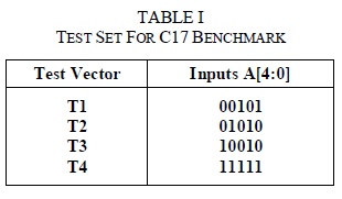 |
| Starting from this deterministic test set, in order to apply the 3-weight test pattern generation scheme, one of the schemes proposed in [5], [8], and [9] can be used. According to these schemes, a typical weight assignment procedure would involve separating the test set into two subsets, S1 and S2 as follows: S1 = { T1, T4 } and S2 = { T2, T3 }.The weight assignments for these subsets is W(S1) = {−, −, 1, −, 1} and W(S2) = {−, −, 0, 1, 0}, where a “−” denotes a weight assignment of 0.5, a “1” indicates that the input is constantly driven by the logic “1” value, and “0” indicates that the input is driven by the logic “0” value. In the first assignment, inputs A[2] and A[0] are constantly driven by “1”, while inputs A[4], A[3], A[1] are pseudo randomly generated (i.e., have weights 0.5). Similarly, in the second weight assignment (subset S2), inputs A[2] and A[0] are constantly driven by “0”, input A[1] is driven by “1” and inputs A[4] and A[3] are pseudo randomly generated. |
| These reasoning calls for a configuration of the accumulator, where the following conditions are met: 1) an accumulator output can be constantly driven by “1” or “0” and 2) an accumulator cell with its output constantly driven to “1” or “0” allows the carry input of the stage to transfer to its carry output unchanged. This latter condition is required in order to effectively generate pseudorandom test patterns in the accumulator outputs whose weight assignment is “−”. |
DESIGN METHODOLOGY |
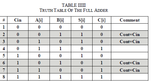
| The implementation of the weighted-pattern generation scheme is based on the full adder truth table, presented in Table II. From Table II we can see that in lines #2, #3, #6, and #7 of the truth table, Cout = Cin. |
 |
| Therefore, in order to transfer the carry input to the carry output, it is enough to set A[i] = NOT (B[i]). The proposed scheme is based on this observation. The implementation of the proposed weighted test pattern generation scheme is based on the accumulator cell presented in Fig. 1, which consists of a Full Adder (FA) cell and a D-type flip-flop with asynchronous set and reset inputs whose output is also driven to one of the full adder inputs. |
 |
| In Fig. 1, we assume, without loss of generality, that the set and reset are active high signals. In this figure the respective cell of the driving register B[i] is also shown. For this accumulator cell, one out of three configurations can be used, as shown in Fig. 2. |
| In Fig. 2(a) we present the configuration that drives the CUT inputs when A[i] = 1 is required. Set[i] = 1 and Reset[i] = 0 and hence A[i] = 1 and B[i] = 0. Then the output is equal to 1, and Cin is transferred to Cout. In Fig. 2(b), we present the configuration that drives the CUT inputs when A[i] = 0 is required. Set[i] = 0 and Reset[i] = 1 and hence A[i] = 0 and B[i] = 1. Then, the output is equal to 0 and Cin is transferred to Cout.. In Fig. 2(c), we present the configuration that drives the CUT inputs when A[i] = ‘−’ is required. Set[i] = 0 and Reset[i] = 0. The D input of the flip-flop of register B is driven by either 1 or 0, depending on the value that will be added to the accumulator inputs in order to generate satisfactorily random test patterns to the inputs of the CUT. |
 |
| In Fig. 3, we present the general configuration of accumulator based 3-weight test pattern generation scheme. The Logic module provides the Set [n-1:0] and Reset[n-1:0] signals that drive the S and R inputs of the Register A and Register B inputs. Note that the signals that drive the S inputs of the flip-flops of Register A, also drive the R inputs of the flip-flops of Register B and vice versa. |
 |
COMPARISONS |
| In Section IV-A, we shall compare the proposed scheme with the accumulator based 3-weight generation scheme that has been proposed in [11]. In Section IV-B, we shall compare the proposed scheme with the 3-weight scan schemes that have been proposed in [5] and [8]. In Section IV-C, in order to demonstrate the applicability of the proposed scheme we shall compare the proposed scheme with the accumulator based test pattern generation scheme proposed in [22]. |
| A. Comparisons with [11] |
| The test application algorithms that have been invented and applied by previous researchers, e.g., [5], [8], [9] can be equally well applied with both implementations based on the number of test patterns applied by [11]. Therefore, the comparison will be performed based on: 1) the hardware overhead and 2) the impact on the timing characteristics of the adder of the accumulator. Both schemes require a session counter in order to alter among the different weight sessions; the session counter consists of log k bits, where k is the number of test sessions (i.e., weight assignments) of the weighted test set. The scheme proposed in [11] requires the redesign of the adder; more precisely, two NAND gates are inserted in each cell of the ripple-carry adder. In order to provide the inputs to the set and reset inputs of the flip flops, decoding logic is implemented, similar to that in [8]. For the proposed scheme, no modification is required for the adder of the accumulator. Therefore, there is no impact on the data path timing characteristics. |
 |
| In Table III we present comparison results for some of the ISCAS’85 benchmarks. In the first column of Table III, we present the benchmark name; in the second and third columns we present the hardware overhead of the accumulator based scheme proposed in [11] and in this work, respectively; in the fourth column we present the decrease of the proposed scheme over [11]. In the fifth through the seventh columns, we present the delay of the adder in terms of number of gates that the carry signal has to traverse, from the Cin input of the adder (lower stage full adder cell) to the Cout output (higher stage full adder cell), as well as the respective decrease obtained by the proposed scheme. In Table III, the hardware overheads are calculated in gate equivalents, where an n -input NAND or NOR accounts for 0.5 n gates and an inverter accounts for 0.5 gates, as proposed in [8]. To calculate delay in the adder operation (columns under heading “#gates from Cin to Cout”) we have to consider the both ripple carry adder and prefix adder implementations. To compare the ripple carry adder implementations, the adder cell used in [11] is considered; in the cell presented in [11], initially the delay from the Cin to Cout of the adder cell is two NAND gates and one XOR gate; in the modified cell proposed in [11], the delay is increased to three NAND and one XOR gate; we have considered that the delay of a NAND gate is one gate equivalent, while the delay of an XOR gate is two gate equivalents. Since the implementation of the proposed scheme does not based on a specific adder design, the utilization of a prefix adder can result in impressive results. To calculate the delay of prefix adders, the formula obtained by [29] is used, where the delay is of the order 4×log n, where n is the number of the adder stages. From Table III, we can see that the proposed scheme results in 57%–90% decrease in hardware overhead, while at the same time it achieves decrease in operational delay overhead that ranges from 84% to 97% for the considered benchmarks. |
| B. Comparisons with Scan-Based Schemes [5], [8] |
| In the 3-weight pattern generation scheme proposed by Pomeranz and Reddy in [5] the scan chain is driven by the output of a linear feedback shift register (LFSR). Logic is inserted between the scan chain and the CUT inputs to fix the outputs to the required weight (0, 0.5, or 1). In order to implement the scheme [5], a scan-structure is assumed. Furthermore, an LFSR required to feed the pseudorandom inputs to the scan inputs is implemented (the number of LFSR stages is log n, where n is the number of scan cells), as well as a scan counter, common to all scan schemes. A number of 3-gate modules is required for every required weighted input (in [5, Table V] and the hardware overhead is calculated for the ISCAS’85 benchmarks). |
| Wang [8] proposed a low overhead 3 weight random BIST scheme, again based on scan chains. He proposed two schemes, namely serial fixing BIST and parallel fixing BIST. Serial fixing scheme presents to be more costly [8]; therefore here we shall concentrate on the parallel fixing BIST scheme. For an n-input CUT and, assuming the availability of the scan chain, the hardware overhead, apart from the LFSR to generate the pseudorandom inputs and the scan counter, includes a decoding logic. The hardware overhead of the decoding logic for some of the ISCAS benchmarks is calculated in [8, Table I]. All schemes requires the application of the session counter, required to alter among the different weight sessions. Schemes proposed in [5] and [8] are test per scan schemes, and, also, assume the existence of scan capability of the latches of design. In Table IV, we have shown arithmetic results for some of the ISCAS’85 benchmarks. |
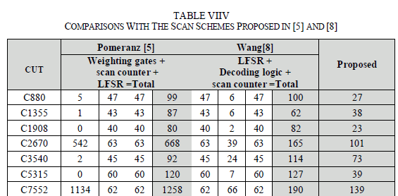 |
| For the calculations in Table IV, we have assumed that schemes [5] and [8] are applied to a circuit with scan capability; therefore, the hardware overhead to transform the latches into scan latches is not considered. For the scheme proposed in [5], the total hardware overhead includes the hardware for the weighting gates (second column), scan counter and LFSR implementation. For the calculation of the numbers in the second column, we used the data found in [5, Table V]. For the scheme in [8], LFSR, scan counter and the decoding logic are considered; the hardware overhead for the decoding logic has been taken from [8, Table I]. |
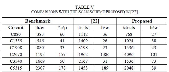
| C. Comparisons With [22] |
| In [22], Manich et al. proposed a methodology to reduce the total test time using an accumulator-based scheme. The scheme operates in test sessions based on triplets of the form (S, I, L), where S is the starting value of the accumulator, I is the increment, and L is the number of cycles the increment is applied before going to the next session. |
 |
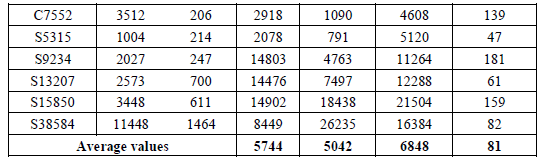 |
| For the comparisons we have utilized the data from [22, Table I], and we have considered that the seeds are stored in a ROM; to calculate hardware, we have considered that a ROM bit is equivalent to ¼ gates, that has been also considered in [20] and [32]. The comparison data for some of the ISCAS’85 and ISCAS’89 benchmarks are presented in Table V, where the same fault coverage, i.e., 100% is targeted. |
| In Table V, the first three columns present the benchmark characteristics (name, hardware overhead in gates, and number of inputs). In the two columns to follow, we present the number of tests required for the scheme in [22], and the respective hardware overhead in gate equivalents. Next, we present the number of test patterns and hardware overhead for the proposed scheme. From Table V, the proposed scheme presents decrease in the hardware overhead, while the number of tests is comparable, while in some cases it also outperforms the scheme in [22]. Here note that the hardware overhead (with respect to the hardware overhead of the benchmarks) is practical, in contrast to [22] which sometimes exceeds the benchmark hardware (c2670, s5378, s9234, s13207, s15850, s38584). It is also interesting to note that the average values in the last line of the Table V. The average increase in the number of tests is 19%, while the average decrease in hardware overhead is 98%. |
CONCLUSION |
| We have presented an accumulator-based 3 weight (0, 0.5, and 1) test-per-clock generation scheme, which can be utilized to efficiently generate weighted test patterns without any modification in the structure of the adder design. Comparisons with a previously proposed accumulator based 3 weight pattern generation technique [11] indicate that the hardware overhead of the proposed scheme is lower (≈75%), while at the same time no redesign of the accumulator is imposed, thus resulting in reduction of 20%–95% in test application time. Comparisons with scan based schemes [5], [8] show that the proposed schemes results in lower hardware overhead. Finally, comparisons with the accumulator based scheme proposed in [22] reveal that the proposed scheme results in significant decrease (≈98%) in hardware overhead. |
ACKNOWLEDGMENT |
| We thank to Dr.A.K. Kureshi, Prof.V.S.Dhondge & Prof. V.G.Puranik of E&TC Dept., Vishwabharti’s Academy College of Engg.,Ahmednagar, for their contribution of this work. |
References |
|