International Journal of Innovative Research in Science, Engineering and Technology
ISSN ONLINE(2319-8753)PRINT(2347-6710)
ISSN ONLINE(2319-8753)PRINT(2347-6710)
S.MUTHARASI1, G.VARATHAN2,
|
| Related article at Pubmed, Scholar Google |
Visit for more related articles at International Journal of Innovative Research in Science, Engineering and Technology
In this project, a three phase indirect matrix converter (MC) is proposed, which can able to generate three-phase ac output voltage with variable magnitudes and frequencies from a fixed three-phase ac power supply. It provides sinusoidal input and output current with bidirectional power flow. Moreover, it allows high reliability, a long life-time, as well as a compact design due to the absence of a bulky electrolytic capacitor. The voltage transfers ratio is limited to less than one in conventional IMC. This problem is overcome by AC boosting function in the proposed one. The proposed topology is simulated using MATLAB/Simulink package and implemented using MOSFET with ATmega16 controller. The simulation and implementation result shows the performance of the proposed converter.
Keywords |
| Common-mode voltage, indirect matrix converter, space vector modulation, voltage transfer ratio |
INTRODUCTION |
| As demand for energy savings have increased in recent years, inverters are being used in a wide range of applications. Demands for lower cost, smaller size and higher efficiency will continue to further expand the range of inverter applications. However, as an attempt toward eco-friendly products increases, some sort of measures is necessary to suppress the harmonics contained in the inverter input current. |
| A matrix converter capable of converting an input voltage directly into an arbitrary AC voltage, instead of converting that voltage into a dc voltage as an inverter shown in Fig.7.This matrix converter has higher efficiency, smaller size; longer lifespan and fever input current harmonics than inverters and has high potential for realizing the above mentioned demands. This paper presents matrix converter and the new technologies that enable its practical application. |
| The matrix converter uses bidirectional fully controlled switches for direct conversion from ac to ac.The nine bidirectional switches are so arranged that any of three input phase could be connected to any output phase through the switching matrix symbol in Fig. 1(a). The matrix converter has some advantages (1) inherent bidirectional power flow (2) sinusoidal input-output waveforms with moderate switching frequency (3) possibility of compact design due to absence of dc-link reactive components. However, the practical applications of the matrix converters are very limlited.The main reasons are (1) complex control of law implementation (2) an intrinsic limitation of the output-input voltage ratio (3) commutation protection of the switches. With space vector PWM control using over modulation the voltage transfer ratio may be increased to 1.05 the expense of more harmonics and large filter capacitiors.In this case, the MC topology used for universal power conversion such as: AC/DC, DC/AC, DC/DC, AC/AC without any change of topology is used [20]-[21],[26]. For three phase AC/AC converter its equivalent circuits combining current source rectifier &voltage source inverter connected by dc link [1]-[3]. |
| Fig.1 (a), (b) shows the circuit configuration of a matrix converter. The inverter is a well-known device that converts an input ac voltage into a dc voltage by a rectifier, and then controls the semiconductor switch of a PWM inverter to convert the DC voltage into the desired AC voltage. A voltage smoothing capacitor required in the DC link circuit, and an electrolytic capacitor is typically used for this purpose. |
| On the other hand, the matrix converter arranges semiconductor switches into a matrix configuration and controls them to convert an input AC voltage directly into the desired AC voltage. Since the input AC voltage is not converted to DC voltages, there is no need for an energy storage device such an electrolytic capacitor. |
| The principle of this control strategy is based on virtual dc-link in matrix converter. This DC link is not physically presented, but the switches are divided to the virtual rectifier and virtual inverter on the Fig .1(b). The indirect space vector modulation is used as a standard technique the matrix converter modulation. Fig. (2) Explains the proposed method of IMC. |
 |
CONVENTIONAL METHODS |
| Nevertheless, an improperly designed modulation strategy will introduce many problems into the system, including common-mode interference [6], waveform distortion caused by narrow pulses, switching losses, etc. The common-mode voltage (CMV) with a high magnitude, a high frequency and a high variation ratio produced by power converters can cause early motor winding failures and bearing deterioration, reduce the lifetime of the winding insulation, break the motor insulation easily, and cause wideband electromagnetic interference on the output side. Thus it is very important to reduce the CMV or limit it within certain bounds for adjustable speed drive systems or other types of loads. Several methods to reduce common-mode voltage have been proposed [6]-[9]. However, these methods were established for matrix converters with an AC output. |
| The first relevant modulation method for the IMC is the standard SVM method, which is presented in [11]- [13]. However, the CMV reduction is not considered in these researches. The standard SVM method provides the peak CMV equal to the input phase voltage magnitude. In [10], [15] two modulation methods are proposed to reduce CMV for IMC. The first method uses the highest and medium line-to-line input voltage to generate the dclink voltage and four active vectors are used in the inverter stage to generate the reference output voltage vector. The maximum voltage transfer ratio is unaffected and remains at 0.86. However, this method has some drawbacks such as the high total harmonic distortion in line-to-line output voltage and the high switching losses in the inverter stage. The second one uses the smallest and medium line-to-line input voltage to generate the dclink voltage and also considers the zero vectors in the inverter stage. The advantage of this method is the high performance at output voltage. However, it allows a maximum voltage transfer ratio of 0.5. |
 |
| In the case of high voltage transfer ratio requirement, in order to overcome the drawback of the conventional method [14]. This paper proposes a new SVM method to reduce CMV which improves the accuracy of synthesizing the reference output voltage and reduces the number of switching states in the inverter stage. The proposed method is based on the use of three instead of four active vectors, as used in the conventional method or two active vectors and two zero vectors as used in the standard SVM method in order to generate the reference output voltage vector[10],[16]. Due to the lack of zero space vectors in synthesis of reference output voltage vector in the new SVM method, the four-step voltage-based commutation is applied in the rectifier stage instead of the zero dc-link current commutation in order to avoid short circuit input lines and open circuit output lines[4],[17], [26]. |
| This paper begins by analyzing CMV and reviewing previous modulation methods for the IMC. Then, the proposed SVM method is presented. The effect of the proposed method on the output performance and a comparative evaluation are also discussed. The voltage transfer ratio successfully improved to 0.95 through this solution. But, the output currents contain large distortions. A matrix converter system is compared to a conventional system that uses a PWM rectifier and inverter. The conventional system needs a capacitor, reactor where as IMC system, needs only a main unit reactor. Therefore, the configuration becomes simple and panel size of the system can be reduced by ½ or more. In addition ,sine the IMC uses one-stage AC-AC direct conversion, thereby low loss system can be realized, achieving at least 1/3 lower loss than in the conventional system [5],[14]. A boost converter is added to the matrix converter leading to improvement of voltage transfer ratio to unity. Simulation results are provided in order to verify the effectiveness of the SVM method. |
PROPOSED TOPOLOGY |
| A new type of AC-DC-AC boost MC (boost matrix converter) based on boost circuit is presented, by connecting a boost circuit operating in the state of high frequency to the middle direct current link of AC-DC-AC matrix converter. The voltage transfer ratio of matrix converter is increased through utilizing the voltage increase function of boost circuit. This new topology is analyzed, and the control strategies of rectifier stage, inverter stage and middle boost circuit are studied. The results indicate that the voltage transfer ratio can be higher than 1.0, the output voltage waveform is very close to standard sine wave, and the harmonic contents increase slightly, which is mainly composed of high harmonics around of switching frequency[14] .The Boost Converter provides a higher output voltage than input voltage. Boost converter topology can be seen in Fig 3. |
 |
| The boost converter also operates in one of two oscillatory modes depending on whether or not switch S is open or closed. These two modes are effectively illustrated below, |
| When switch S is closed, the diode is reversed biased effectively eliminating portion of the circuit and current flows only through the inductor and the switch as shown in Fig .4 (a), (b) .This stores energy in the inductor after a certain time, the switch is turned off and the circuit effectively becomes that shown in Fig.4 (b). The current stored in the inductor then flows through the now forward-biased diode and through the load. Mode ends when the switch is turned on again and the cycle repeats. |
 |
| When a boost converter operates in continuous mode, the current through the inductor (IL) never falls to zero. Fig.4 shows the typical waveforms of currents and voltages in a converter operating in this mode. |
| a. As shown in Fig.5.a, the switches S1, S2 and S3 are on and transfer the converter input line voltage Usa −Usc to the DC-link in analogy to conventional switching strategy of the IMC. In this condition the clamp diode turns on and the clamp capacitor Cc starts charging. |
| b. In step two after the clamp capacitor Cc is charged to the peak of the input line voltage ( 3 (×Usm) the clamp circuit diode turns off. In this step the DC-link voltage is equal to Uac. |
| c. Assume that the line side converter modulation index mi be lower than 1:mi < 1 |
| d. As shown in fig 5.d In this step the switches S1, S2 and S3 are switched on, S4 is switched off while the line voltage, Usb –Usc is transferred to DC-link in analogy to conventional switching strategy of the IMC. Thus, the boosting energy stored in the filter inductors is released to the filter capacitors resulting in an amplified voltage at the input. In this step the DC-link voltage is equal to Ubc [4], [5]. |
 |
 |
| A.SPACE VECTOR PWM |
| The circuit model of a typical three-phase voltage source PWM inverter is shown in fig.6 S1 to S6 are the six power switches that shape the output, which are controlled by the switching variables a, a’, b, b’, c and c’. When an upper switch is switched on, i.e., when a, b or c is 1, the corresponding lower transistor is switched off, i.e., the corresponding a’, b’ or c’ is 0. Therefore, the on and off states of the upper switch S1, S3 and S5 can be used to determine the output voltage [17], [20], [26]. |
| SVPWM is a different approach from PWM modulation, based on space vector representation of the voltages in the α-β plane. The α-β components are found by Clark’s transformation. Space Vector PWM (SVPWM) refers to a special switching sequence of the upper three power transistors of a three-phase power inverter. |
| It has been shown to generate less harmonic distortion in the output voltages and/or currents applied to the phases of an AC motor and to provide more efficient use of dc input voltage. Because of its superior performance characteristics, it has been finding widespread application in recent years. |
 |
| From these two-phase components, the reference vector magnitude can be found and used for modulating the inverter output. The process of obtaining the rotating space vector is explained in the following section, considering the stationary reference frame. Considering the stationary reference frame let the three-phase sinusoidal voltage component be, |
 |
 |
| When this three-phase voltage is applied to the AC machine it produces a rotating flux in the air gap of the AC machine. This rotating resultant flux can be represented as single rotating voltage vector. The magnitude and angle of the rotating vector can be found by means of Clark’s Transformation as explained below, |
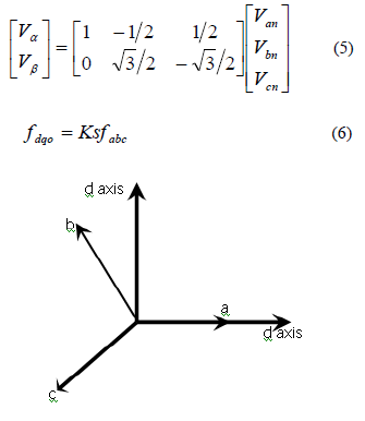 |
| Fig .8 The relationship of abc reference frame And stationary d-q reference frame |
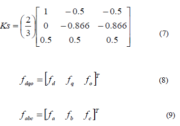 |
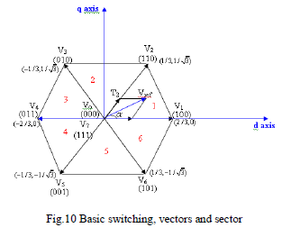
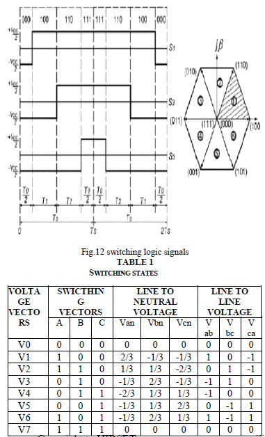
| And f denotes either a voltage or a current variable. As described in fig: 8 this transformation is equivalent to an orthogonal projection of [a b c] t on to the twodimensional perpendicular to the vector [1 1 1] (the equivalent d-q plane) in a three-dimensional coordinate system. As a result, six non-zero vectors and two zero vectors are possible. Six non-zero vectors (V1-V6) shape the axes of a hexagonal as depicted in fig: 9 and supplies power to the load. The angle between any adjacent two non-zero vectors is 60 degrees. Meanwhile, two zero vectors (V0 and V7) and are at the origin and apply zero voltage to the load. The eight vectors are called the basic space vectors and are denoted by (V0, V1, V2, V3, V4, V5, V6, and V7). The same transformation can be applied to the desired output voltage to get the desired reference voltage vector, Vref in the d-q plane. The objective of SVPWM technique is to approximate the reference voltage vector Vref using the eight switching patterns. One simple method of approximation is to generate the average output of the inverter in a small period T to be the same as that of Vref in the same period. |
| Any space vector lies in the hexagon can be composed by time averaging of the adjacent two active space vectors and zero vectors. For each switching period Ts, |
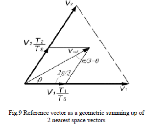 |
| The geometric summing up can be articulated mathematically as |
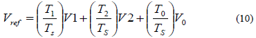 |
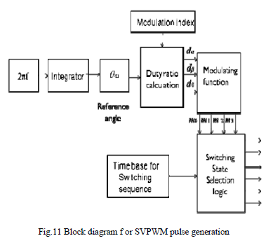
| Where, T1 is the time for which space vector V1 is selected and T2 is the time for which space vector V2 is selected. The block diagram for generating SVM pulses is shown in Fig.6. For 180° mode of operation, there exist six switching states and additionally two more states, which make all three switches of either upper arms or lower arms ON. To code these eight states in binary (onezero representation), it is required to have three bits (23 = 8). |
| And also, as always upper and lower switches are commutated in complementary fashion, it is enough to represent the status of either upper or lower arm switches. In the following discussion, status of the upper bridge switches will be represented and the lower switches will it’s complementary. Let "1" denote the switch is ON and "0" denote the switch in OFF. Table: 1 gives the details of different phase and line voltages for the eight states. |
 |
| SVM can be instigated through the following steps: |
| 1. Computation of reference voltage and angle (θ) |
| The space vector, Vref is normally represented in Complex p lane and the magnitude as, |
 |
| 2. Identification of sector numbers |
| The six active-vectors are of equal magnitude and are mutually phase displaced by π/3. The general art isolation can be represented by, |
 |
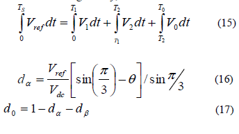
| 3. Calculation of space vector duty cycle |
| The duty cycle calculation is done for each triangular sector formed by two state vectors. The individual duty cycles for each sector boundary state vectors and the zero state vectors are given by, |
 |
 |
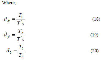 |
| This gives switching times T 0, T1 and T2 for each inverter state for a total switching period, Ts. Applying both active and zero vectors for the t time periods given in (20) ensures that average voltage has the same magnitude as desired. |
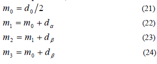
| 4. Calculation of modulating function |
| The four modulating functions, m0, m1, m2 and m3, in terms of the duty cycle for the space vector PWM scheme can be expressed as, |
 |
| 5. Initiation of SVPWM pulses |
| The required pulses can be initiated by comparing the modulating functions with the triangular waveform. A symmetric seven segment technique is to alternate the null vector in each cycle and to contrary the sequence after each null vector. The switching pulse pattern for the 3 phases in the six sectors can be initiated. A typical seven segment switching sequence for generating reference vector in sector one is shown in Fig 12. |
 |
SIMULATION RESULTS |
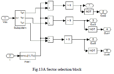
| In order to verify the validity of the topology with the optimized modulation scheme in this paper, the intended inverter is tested with series-connected RL load. The load resistor is RL and the load inductor is LL. A three-phase inverter with a balanced star connected RL load is considered. A complete mathematical model of the SVPWM is developed and simulated using MATLAB/Simulink to investigate the performance of a three phase inverter.Fig.13Shows the sector selection algorithm. |
 |
| Simulation Results: |
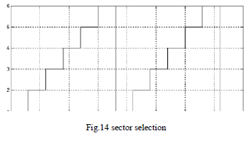
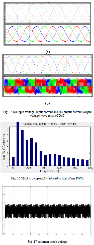
| Sector corresponds to the location of voltage in the circular locus traced by it and is divided into six sectors of 60° each which is shown in Fig. 14 and line voltages, Current are shown in Fig.15 (a),(b). Shows the line current, because of the inductive nature of the load, higher order harmonics have been potable out and the current waveform is sinusoidal in nature. Also there will be reduction in THD when compared to that of the Sin- PWM as shown in Fig.16. Common mode voltage reduced than other conventional method Fig.17. |
 |
 |
CONCLUSION |
| An improved SVM method for IMC is proposed in this thesis to reduce common mode voltage. The proposed topology serves lower THD in line to line output voltage and reduced switching loss in the inverter stage when compared to other conventional methods. The given topological network is simulated in the MATLAB 7.9(R2009b) environment both for existing and proposed method. Originating from the idea of AC boosting function, perfection is brought to the conventional IMC topology with adding four unidirectional switches. A new switching strategy is applied to achieve the boosting function and to reduce the switching losses as well. Simulation results show that for improved SVM method there is a rise in voltage transfer ratio compared to existing method. Since voltage transfer ratio of IMC using SVM method is increased it results in the reduction of THD and improved efficiency. |
References |
|