International Journal of Innovative Research in Science, Engineering and Technology
ISSN ONLINE(2319-8753)PRINT(2347-6710)
ISSN ONLINE(2319-8753)PRINT(2347-6710)
P.Narmatha1, M.N.Vanitha Devi2, A.Jagadeeswaran3
|
| Related article at Pubmed, Scholar Google |
Visit for more related articles at International Journal of Innovative Research in Science, Engineering and Technology
Flip-flops are the major storage elements in all SOC’s of digital design. They accommodate most of the power that has been applied to the chip. Flip-flop is one of the most power consumption components. It is important to reduce the power dissipation in both clock distribution networks and flip-flops. The power delay is mainly due to the clock delays. The delay of the flip-flops should be minimized for efficient implementation. The concept of this project is to reduce the power consumption and to increase the speed and functionality of the chip. This project moves around in replacing conventional master-slave based flip flop to a pulse triggered flip flop which acts as a tribute alternate for low power applications. Initially in the critical path the pulse generation controls logic along with SVL function. A simple transistor SVL design is used to reduce the circuit complexity. In this scheme transistor sizes and pulse generation circuit can be further reduce for power saving. Here UMC CMOS 180nm technology is use in SPICE tool to design the proposed structure. This would bring up the result in power saving approximately to 38.4%.
Keywords |
| Flip-flop, low power, svl. |
INTRODUCTION |
| Flip-Flops and latches are the basic elements for storing information. One latch or Flip-Flop can store one bit of information. The main difference between latches and flip-flops is that for latches, their outputs are constantly affected by their inputs as long as the enable signal is asserted. In other words, when they are enabled, their content changes immediately when their inputs change. Flip-flops, on the other hand, have their content change only either at the rising or falling edge of the enable signal. This enable signal is usually the controlling clock signal. After the rising or falling edge of the clock, the flip-flop content remains constant even. |
| If the input changes. There are basically four main types of latches and flip-flops: SR, D, JK, and T.The major differences in these flip-flop [13] types are the number of inputs they have and how they change state. For each type, there are also different variations that enhance their operations. Figure 1(a), (b) illustrates the difference between positive edge triggered flip flop and an active high latch. As it can be seen in this figure, possible changes of input can be seen at the output of the latch while it is transparent |
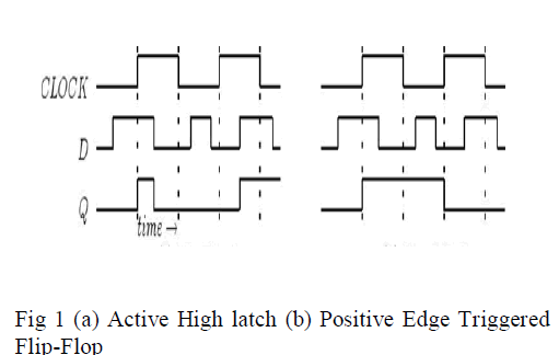 |
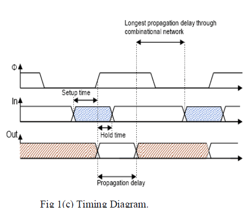
| The performance of a flip-flop is measured by three important timings and delays: propagation delay (Clock-to-Output), setup time and hold time. They reflect in the system level performance of the Flip-Flops [5]. Setup time and hold time define the relationship between the clock and input data as shown in the Figure 1(c) |
| Setup time and hold time describe the timing requirements on the D input of a Flip-Flop with respect to the Clk input. Setup and hold time define a window of time which the D input must be valid and stable in order to assure valid data on the Q output. Setup Time (Tsu) – Setup time is the time that the D input must be valid before the Flip-Flop samples. Hold Time (Th) – Hold time is the time that D input must be maintained valid after the Flip-Flop samples. Propagation Delay (Tpd) – Propagation delay is the time that takes to the sampled D input to propagate to the Q output. |
 |
II. TECHNIQUES FOR IMPLEMENTING IMPLICIT PULSE-DATA CLOSED TO OUTPUT TRIGGERED FLIP-FLOPS |
| Implicit pulse generation is often considered to be more power efficient than explicit pulse generation. This is because the former merely controls the discharging path while the latter needs to physically generate a pulse train. Implicit-type designs, however, face a lengthened discharging path in latch design, which leads to inferior timing characteristics [1]. |
| In digital circuit design, large proportion contributes to synchronous design and they are operated based on the clock signal to reduce the complexity of the circuit design. In the design of sequential circuits, a major challenge is the design of an efficient D flip-flop (DFF). Several static/dynamic DFF architectures have been proposed in [1]-[10]. The topology comparison commences with the conventional single edge triggered flip-flop SET [1] typically latch data either at the positive or negative edge of the clock. A SET FF can be configured to operate as master slave latch by cascading the sequential structure but it is incompetent as half of the clock edges are wasted, while the full implementation cost of the complete clock is endured. Next topology is Double Edge Triggered flip-flop DET, which can be triggered at the positive as well as the negative edges. |
| The implicit type flip-flop generates the pulse inside the flip-flop. The circuit diagram of ip-DCO is shown in the Figure 3.1. In ip-DCO the clock signal and complement of the clock signal generates a narrow pulse of short pulse width [6]. During this pulse the output follows the input. First, during the rising edge, nMOS transistors N2 and N3 are turned on. If data remains high, node x will be discharged on every rising edge of the clock. This leads to a large switching power. The other problem is that node x controls two larger MOS transistors (P2 and N5). The large capacitive load to node x causes speed and power performance degradation. When the x as denoted floating node, |
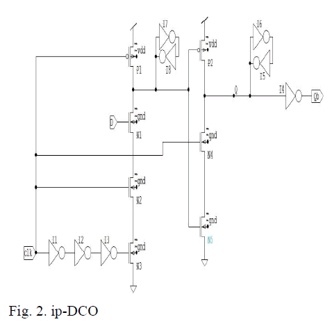 |
| The node x controls two larger transistors P2 and N5, this leads to large capacitive load to node x causes power performance degradation. Fig. 3 shows the simulation waveforms of the proposed P-FF design against the MHLLF design. |
SCCER |
| In this design shown in fig 3, a weak pull up transistor P1 is employed in conjunction with an inverter I2 to reduce the load capacitance of node. The discharge path contains NMOS transistors N2 and N1 connected in series. In order to eliminate superfluous switching at node X, an extra NMOS transistor N3 is employed. Since N3 is controlled by Q_fdbk, no discharge occurs if input data remains high. |
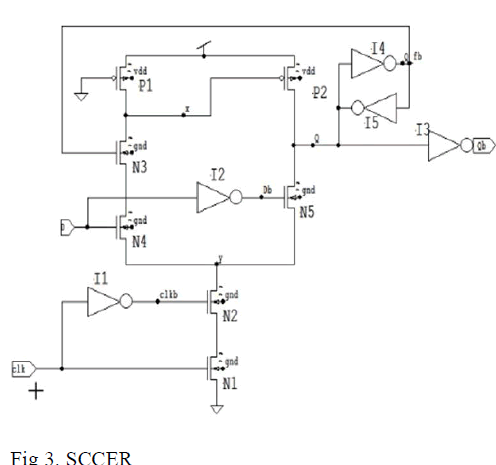 |
| The worst case timing of this design occurs when input data is “1” and node X is discharged through four transistors in series, i.e., N1 through N4, while combating with the pull up transistor P1. |
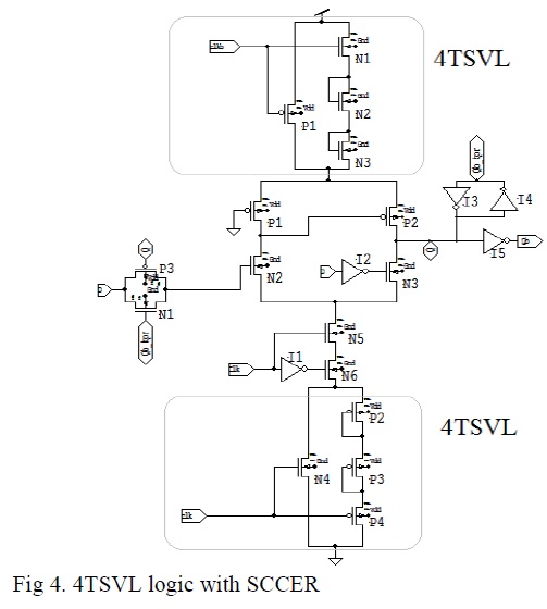
B.4TSVL with SCCER |
| In order to avoid that we can incorporate the leakage reduction circuit called “Self-Controllable Voltage Level Circuit to this flip flop to reduce the power consumption. The block diagram of SVL-flip flop is shown in figure 4. The two circuits called upper SVL (U-SVL) and Lower SVL (L-SVL) is used to construct the above fourth proposed flip flop. Upper SVL consists of one PMOS (pSW) act as a switch and multiple NMOS (nRSm) act as resistors connected in series. Similarly, Lower SVL constructed by one NMOS (nSW) and multiple PMOS (pRSm) in series. |
| clk=1 and clkb=0, P3 and N6 is ON but N4 and P5 is OFF. Therefore the Upper and Lower SVL blocks can supply a maximum supply voltage Vdd and a minimum ground level Vss respectively. While the stand-by mode i.e clk=0 and clkb=1, P3 and N6 is OFF but N4 and P5 is ON. Upper SVL circuit generate lower supply Vdd (=Vdd-Vn<Vdd) to a flip flop and Lower SVL circuit gives higher ground level voltage Vss (=Vp>0). Where Vn and Vp is the total voltage drop of N4, N5 and P4, P5 respectively. In this mode the back-gate bias (VBGS) of the P3 and N6 are increased. Then Vts of P3 and N6 also increases. Thus, the leakage current and power is decreases. Finally the total power consumption of flip flop is reduced. |
 |
III.SIMULATION RESULTS |
| The simulation results were obtained from TSPICE in 180nm CMOS process at room temperature VDD is 1V. All flip flops were simulated with output load capacitance Cload and layout level. Following flip flop metrics are carried out to compare the performance flip flops. |
| Total no of Transistors: The total number of transistors is measured which contribute more area and power consumption in the integrated circuit design. |
| Power: It is the total power consumption of flip flop in terms of μw (micro watt).the maximum power denotes the maximum power consumption of flip flop. The minimum power describe the minimum power requirement to trigger the flip flop |
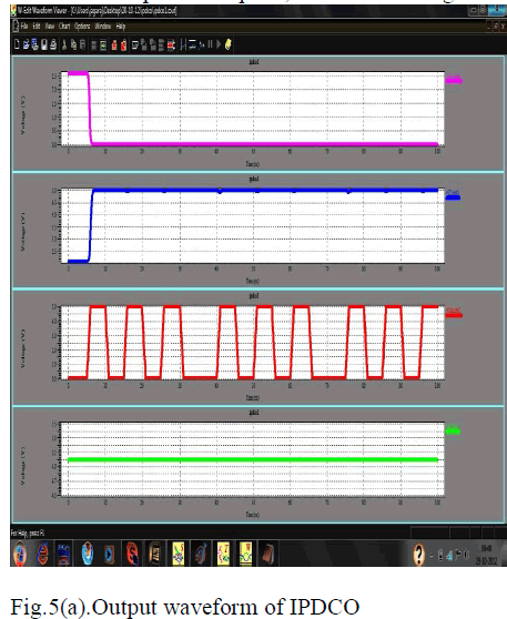
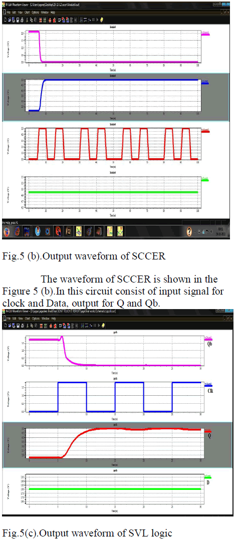
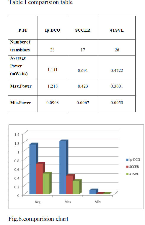
| To illustrate the merits of the presented work, Fig. 5 shows the simulation waveforms by using T-Spice tool. Fig 5(a) describe the output waveform obtain for IPDCO .Fig 5(b) describes the output curve of SCCER flip flop.Fig5(c) shows the performance curve of proposed flip flop with SVL logic. |
| Table I summarizes some important performance indexes of these P-FF design. These include transistor count, average power, maximum power, minimum power and the simulation time. |
| Fig 6 shows the comparison chart of three flip flops which denotes the average power, maximum power and the minimum power of ipdco, sccer and svl logic. |
 |
| When the data is apply ‘1’ at the time of clock as rising edge, then the output of Q is ‘1’ because it act as the D flip flop operations. |
 |
| When the fig 5(c) shows that operation of the SVL logic output and performed D flip flop,initially clk=0,what ever input does not consider the output ‘0’ Table I comparision table |
| When the fig 5(c) shows that operation of the SVL logic output and performed D flip flop,initially clk=0,what ever input does not consider the output ‘0’ |
 |
IV.CONCLUSION |
| In this project, the various Flip flop design like, ip-DCO, MHLFF, SCCER and Proposed flip-flop design with pulse control scheme are discussed. These flip-flop were been designed in Tanner tool and the results and waveforms are also obtained. The comparison table also added to verify the designed methods. Even though, when the circuit is in idle condition the circuit consumer some power which is said to be leakage power.A master slave flip flop is initially replaced with pulse triggered flip flop and a simple SVL logic is used to reduce the power consumption and increase the device functionality. The result and the comparison chart describe that the SVL logic increased the performance of flip flop. |
References |
|