International Journal of Innovative Research in Science, Engineering and Technology
ISSN ONLINE(2319-8753)PRINT(2347-6710)
ISSN ONLINE(2319-8753)PRINT(2347-6710)
| Iqbal S. Naji Assistant Professor, Department of Physics, College of Science, University of Baghdad, Baghdad, Iraq |
| Related article at Pubmed, Scholar Google |
Visit for more related articles at International Journal of Innovative Research in Science, Engineering and Technology
n-type CdSexS1-x thin films of 500nm thickness with various Se content (0, 0.4, 0.8 ,& 1) were deposited on monocrystalline p-type Si (111) substrate at room temperature with rate equals to 9.25 A/sec by thermal evaporation technique. The effect of compound concentration (Se content) on the electrical properties of CdSexS1-x/Si heterostructure diodes was studied. The capacitance- voltage characteristic at frequency equal to 1 MHz revealed that these diodes are abrupt type, and the capacitance increases with increase Se content, while the width of depletion layer decreases. The current-voltage measurement for CdSexS1-x/Si diodes shows that the forward current at dark condition varies approximately exponentially with applied voltage and the mechanism of transport current coincide with diffusiontunneling model. The ideality factor decreases , while the tunneling constant increases with increasing Se content. The I-V measurements under illumination shows that the photocurrent increases with increasing Se content.
Keywords |
| CdSexS1-x alloys and films, thermal evaporation technique, C-V characteristics of CdSexS1-x/Si heterojunction, I-V characteristics of CdSexS1-x/Si heterojunction. |
INTRODUCTION |
| II-VI composite semiconducting chalcogenides, especially sulfides and selenides have been investigated extensively, owing to their interesting opto-electronic properties. These compound semiconductors are widely used in solid-state such as infrared detector, photovoltaic cells, nuclear radiation detector and windows for infrared laser [1]. The addition of CdSe to CdS has resulted a solid solutions called cadmium sulfo-selenides (CdSSe) . They appear very promising for various practical applications . To a great extent, these expectations are based on the possibility of controllable changing of important parameters (lattice constants, band gaps, etc). The band gap of CdSexS1-x crystal changes continuously with the composition (x) with in the energy range corresponding to the visible wavelengths [2]. CdSeS having specific physical properties such as direct band gap widths, high absorption coefficients in the visible and infrared part of the solar spectrum, good electrical properties (e.g carrier mobility and lifetime ) and increased capability in obtaining adjustable n-or p-type conductivity by doping [3,4] Cadmium sulphoselenid is widely used as semiconducting material, mainly as photoconductors, but with increasing interest focused on their use in photovoltaic, photoelectrochemical devices, solar cells, light emitting diodes, discrete and multi element photo resistors, optical filters, signal memory devices, laser screens, infrared imaging devices, optoelectronic switches, linear image sensor for digital facsimile page scanners, electrophotography, image intensifiers and exposure meters [1,5]. Several techniques were employed for the growth of thin films of the ternary CdSSe such as thermal evaporation [6,7], laser ablation technique [8,9], sputtering [10], brush plating technique [11], chemical bath deposition [12,13], electron beam [14]. In the present work, CdSexS1-x films were deposited by thermal vacuum evaporation using the powders synthesized in our laboratory on single crystal Si as substrate and study the electrical properties of these heterojunctions. |
II. EXPERIMENTAL PROCEDURE |
| CdSexS1-x alloys of different x values (0, 0.4, 0.8 ,& 1) were prepared from appropriate atomic percentages with high purity elements(99.99%) obtained from Switzerland. |
| An isotype CdSexS1-x /Si heterojunctions were made by depositing n-type CdSexS1-x films of thickness equal to 500 nm with rate equals to 9.25 A/sec by thermal resistive technique under pressure of 8x10⁻⁶ mbar on p-type monocrystalline silicon wafer have orientation (111) as a substrate . The Si substrates are dipped in diluted HF acid for 20 sec and then in DI water rinse. Ohmic contacts are made on both CdSeS film and Si substrate by depositing of Ag and Al films through certain mask. The capacitance-voltage characteristics of the heterojunctions were measured using LRC apparatus type (Agileut 429 uA Precision Impedance Analyzet) at frequency 1 MHz . Capacitance at different reverse bias voltage at the range (0-1) volt was measured to determine the type of the heterojunction (abrupt or graded), and the value of built-in voltage (VD) was obtained from the intercept at (1/C2)=0 by extrapolating the curve to the voltage axis. Also the width of the junction can be deduced from the flowing equation [15] |
| Where Co is the capacitance at zero biasing voltage, and |
 |
| Where ÃÂÃâs is the semiconductor permittivity for the two semiconductor materials. The concentration of carrier was calculated from the relation [16] |
 |
| Where [2(ÃÂÃâ1NA1+ ÃÂÃâ2ND2)/qND2NA1ÃÂÃâ1 ÃÂÃâ2] represent the slope, NA1 and ND2 are the accepter and donor concentrations, and ÃÂÃâ1, ÃÂÃâ2 are the dielectric constant of p-type and n-type semiconductor respectively. VD is the built-in potential, Va is the applied voltage. |
| The response and rise time can be found from the flowing equations |
| tresponse = t r /2.2 ………………………………………….....…(4) |
| Where |
| tr= RC ……………………………..………………..………...(5) |
| The dark current-voltage measurement for CdSexS1-x/Si were carried out by using applying a voltage to the sample from a stabilized d.c fine power supply. The current passing through the device was measured using digital electrometer (Keithley 616). The bias voltage was varied (0-5) Volt in the case of forward and reverse bias. From the plot of the relation between forward current and bias voltage in the dark the ideality factor was determined from the relation [17] |
 |
| The tunneling constant ̉̉ was deduced from equation: |
| While the rectification factor (RF) was calculated according to the following equation [18] |
| In the light condition, the optoelectronic measurements of diodes were made, the samples were exposed to halogen lamp at intensity equal to (70) mW/cm2. |
III. RESULTS AND DISCUSSION |
| The capacitance – voltage characteristics of CdSexS1-x/Si heterojunction with different x values (0, 0.4, 0.8 , 1) achieved in frequency equals to 1 MHz are shown in figure (1) . This measurement was studied in order to get an idea about the impurity distribution in the vicinity of the junction. The capacitance is expected to decrease with increasing reverse bias, due to an increase in the depletion region width ,and it is clear from this figure the reduction was non-linear. Additionally, it can observed that the capacitance at zero bias voltage (Co) was increase from 0.098 to 0.169 nF when x content change from zero to one . This could be attributed to increase the carrier concentration when Se content increases in the CdSexS1-x composition , which leads to increase the capacitance and as a result the depletion region width decreases, this means the carrier of CdSexS1-x films have more diffusion when the Se content decreases. The width of the depletion layer (W) has a large value when the Se content decreases to zero. Figure (2) reveals the reciprocal of square capacitance versus reverse bias voltage. The linearity characteristic of this plot confirms that the junction is abrupt type. From the intercept on the x-axis and the slope of the best fit straight line, the built in voltage and an impurity concentration of donors can be obtained respectively. Table (1) illustrates all the parameters that are calculated from this measurement. The value of built in voltage (VD) increases from 0.50 to 0.53 V with decrease the Se content from 1 to zero except for x=0.8 have a larger value (0.70 V) . This may attributed to appear more than one phase in this ternary compound. |
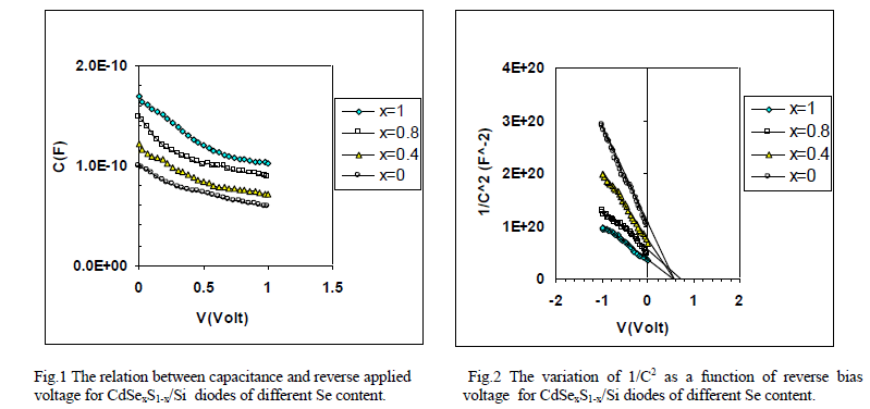 |
| Our result agree with the result of Mousa et al [19] ,they prepared CdS/Si heterojunction by CBD, and found VD equal to 0.6V ,while Ahmed [20] prepared CdSeS/Si heterojunction by thermal evaporation from CdS and Se source .He found high value for VD (1.3V) . Also Ismail et al [21] found high value of VD (1.4V) for CdS/Si heterojunction prepared by spray pyrolysis. |
 |
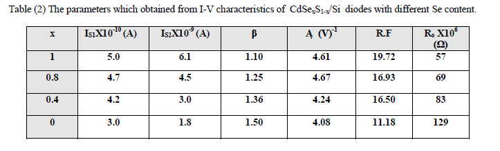
| The carrier concentration of donor (ND) layer of CdSexS1-x/Si heterojunction increases from 0.808x10¹⁴ to 2.031x1014 cm-3 with increasing Se content from zero to one. This behavior was due to the increasing in the depletion region width. Also the rise (tr) and response time (tresp) were calculated as shown in Table (1). More thorough analysis of the current- voltage characteristics is necessary to specify the current mechanisms. A measured current – voltage plot which represent forward and reverse bias voltage under dark condition of an isotype CdSexS1-x /Si heterojunction of different x content is shown in figure (3). From this figure, it is clear that the current increases with increasing Se content, this may be due to improve in the crystal structure that implies the increase in the grain size, and to decrease in the depletion layer as shown in C-V characteristics. The ratio between forward and reverse current at certain applied voltage represents the rectification coefficient (B) has been determined at 2 volt as shown in Table (2). It is obvious that B increases considerably with increasing Se content. This indicate that the CdSexS1-x /Si heterostructures have rectification properties and their electrical characteristics change with increasing selenium contents. |
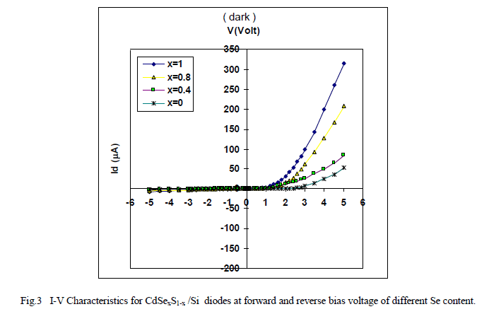 |
| One can easily distinguish two linear regions in the I-V plot. Under forward bias conditions, the current flows relatively freely in this direction of the diode and the resistance of the photodiode is determined by the series resistance (Rs) .Two main components contribute to the resistance, the base layer and the electric contacts).In the reverse bias region, very low current flows, the influence of shunt resistance (Rsh), which is usually similar to the Rmax value, predominates. The main source of the shunt resistance is a surface leakage current connected with the passivation of the junction [22]. In general the forward dark current is generated due to the flow of majority carriers and the applied voltage inject majority carriers which leads to decrease the value of built in potential, and decrease the width of the depletion layer. The majority and minority carrier concentration is higher than the intrinsic carrier concentration (ni), i.e np > ni 2 which is leading to generate recombination current at low voltage region [23].while the tunneling current is represented at high voltage region [24]. The mechanism of transport current is estimated from the value of ideality factor (β) ,where the value of β equals to one, this indicates minority carrier diffusion, while β equals to two is obtained when generation and recombination of electron- hole pairs in the photodiode depletion region determines the forward dark current [22]. |
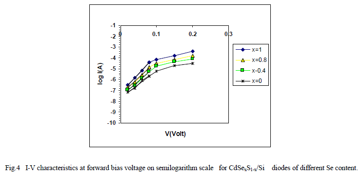
| Figure (4) shows the semi-log of the dark forward current as a function of applied voltage (0-0.2)V for CdSexS1-x /Si diodes of different x values. There are two regions can be recognized in this figure. The ideality factor can be determined from the slope of linear dependence of the first region of log (I) on the forward bias voltage. It is increases from 1.103 to 1.504 when Se content changes from one to zero. This indicates that these devices are almost diffusion limited at room temperature. While from the second region in the same figure, the tunneling constant can be calculated as shown in Table (2). |
 |
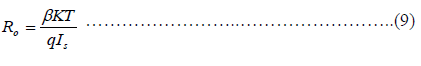
| The ideality factor (β) and the saturation current (Is) can be used to determined the theoretical value of zero- bias resistance (Ro) of the photodiode using a simple formula [22] : |
 |
 |
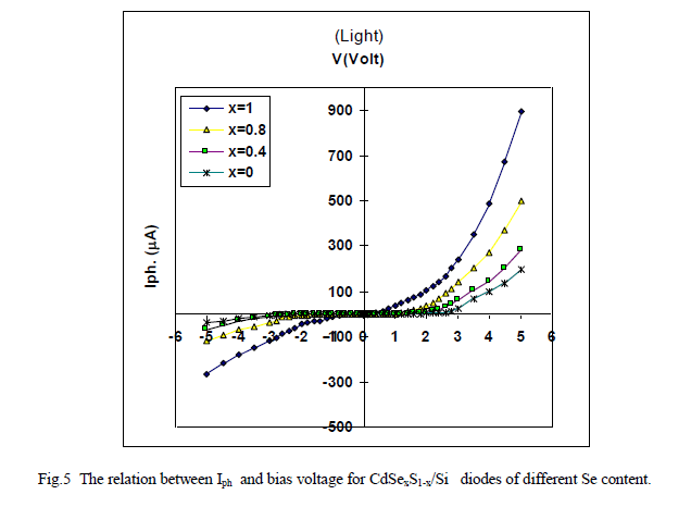
| The variation of the photocurrent (Iph) with the bias voltage (Va) of the CdSexS1-x /Si diodes with different Se content are presented in Fig.(5), the measurements are carried out under illumination power density equal to 70 mW/cm2 at room temperature. From this figure we observe that the photocurrent increases with increasing the bias voltage. This is happened because increasing the electric field sweeps the carriers out of the depletion region and with existing illumination, electron-hole pairs are created near the junction. If the e-h pairs is generated within a diffusion length (Ln, Lp) of the transition region, the electrons can diffuse to the junction and swept down the barrier to the n side. |
| The resulting current is called the generation current since its magnitude depends entirely on the rate of generation of e-h pairs. So that the photocurrent is expressed as function of generation and diffusion mechanism as in the following equation [15]. |
| Where Gph generation rate of photocarriers , Lp and Ln are the diffusion length of holes and electrons, respectively. From the same figure it is clear that the photocurrent increases with increasing x value this is attributed to the decrease of the energy gap with increasing x value. |
 |
IV. CONCLUSION |
| The electrical properties of CdSexS1-x /Si diodes has been analyzed . Capacitance- voltage measurements shows that the impurity profile near the junction is abrupt, and the capacitance increases , while the width of depletion layer decreases with increasing Se content. The mechanism of the current transport in the forward condition coincides with diffusion- tunneling mechanism. It has been found that these diodes have rectification properties, where the rectification coefficient increases with increasing Se content in this compound. The value of ideality factor increases , while the tunneling constant decreases when Se content reduce in the ternary compound. Under illumination condition, the photocurrent increases obviously with increasing Se content. |
References |
|