International Journal of Innovative Research in Science, Engineering and Technology
ISSN ONLINE(2319-8753)PRINT(2347-6710)
ISSN ONLINE(2319-8753)PRINT(2347-6710)
Sunitha M S1, Bharat G Hegde2, Deepakakumar N Hegde2
|
| Related article at Pubmed, Scholar Google |
Visit for more related articles at International Journal of Innovative Research in Science, Engineering and Technology
Building low-power, high speed systems have been in demand, in recent years, because of the fast growing technologies in mobile communication and computation. Arithmetic and Logic Unit is a core component of almost all computing machines and processors. This work involves the design and comparison of 3 different 16 bit RISC processors based on 3 different ALU architectures. The ALU architectures are differentiated based on consumer requirements, keeping in mind cost, speed and power. Comparisons are done on aspects of area occupied, speed and power consumption. The first ALU design is an economical design, less complex and low power. The second design is a high speed, low power model using Carry Look-Ahead Adders (CLAs) and Vedic multiplier. Extensive parallelism is seen in them. The third design is targeted for low power and compactness and uses Prefix adders and Booth multiplier. The design of the RISC processors also involves the design of memory and development of opcodes which are also included in this work. A typical RISC based program on circular convolution has been implemented on all of these for comparison purposes. Results prove that ALU2 is the fastest and also consumes very less power. It is 15% faster than ALU1 but also occupies 20% more area. ALU3 occupies 30% lesser area than ALU1 and is a low power model. Though moderate in performance, ALU1 is the easiest to design.
Keywords |
| ALU, RISC Processor, Pipeline Breakage, Vedic Multiplier, Convolution. |
INTRODUCTION |
| The architecture of ALU has serious impact on timing, power dissipation and area. The power dissipation of the ALU depends mainly on the architecture. The timing and area depends on the type of circuits used to implement the ALU components. The battery technology does not advance at the same rate as the microelectronics technology. So designers are faced with constraints such as high speed, high throughput, small silicon area, and at the same time, lowpower consumption. Hence proper choice of ALU architecture is needed. Although many functions can be performed by ALU, the basic arithmetic operations of addition, subtraction, multiplication, division and simple Boolean operations such as logical and shifting operations continue to be the core operations. An ALU loads data from the input registers or memory. Based on the type of control signal from the control unit, it performs the desired computation on this data and finally stores the result in an output register. The control unit is responsible for moving the processed data between these registers, ALU and memory. A RISC processor is designed to work with a small but powerful set of instructions, with the aim of increasing the throughput of the processor. The main feature of the RISC processor is its ability to support single cycle operation, meaning that the instruction is fetched from the instruction memory at the maximum speed of the memory. The intention of this work was to create the functional units of the RISC processor as building blocks in Verilog HDL [1] since at a high level of complexity it is easier to implement the function in software. After designing different ALU structures, we combine them with memory and register set to perform as a full fledged RISC processor. The different ALU designs are validated by implementation of Circular Convolution on these. The opcodes designed for this purpose are also discussed in this paper. The rest of the paper is organised as follows. Section II briefly describes the design of the 3 ALU architectures. Section III describes the design of the RISC processor. Convolution program implementation is described in Section IV. FPGA implementation and results are discussed in Section V. Section VI concludes the paper. |
II. DESIGN OF ALU ARCHITECTURES |
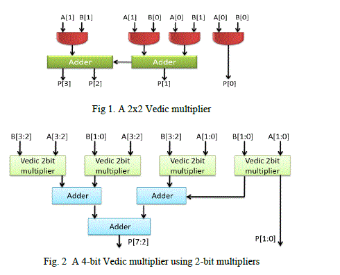
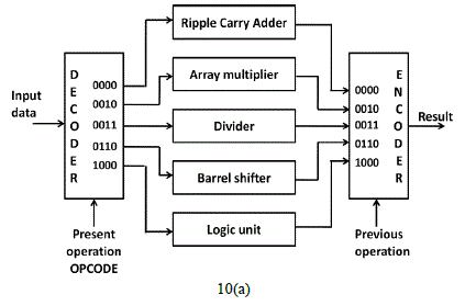
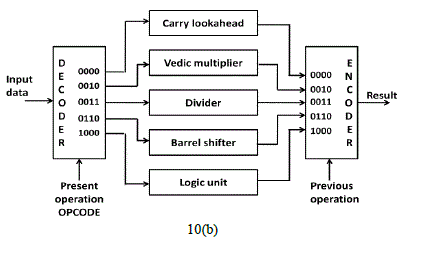
| ALU1 (economical) is built in a simplistic way without tendering to power, delay or area constraints. It consists of a Ripple Carry Adder (16 bit) built with full adders. It's a slow adder as each stage has to wait for the previous carry to occur. The multiplier used is an Array multiplier. This increases the speed in comparison to iterative addition but is still not optimal. A n x n multiplier requires n2 AND gates, n half adders and n x(n-2) full adders. ALU2 (high speed, low power) is built using constraints of parallelism. The Carry Look Ahead adder (CLA) used in this consists of carry generate and propagate terms that are used to precompute the carry thereby increasing its speed [2]. The hardware complexity, though, is very high as can be seen in the results. Hence the area occupied is large. The novelty involved is in the use of Vedic multiplier using Urdhava Triyagbhyam sutra. Further it is known that the conventional Vedic multiplication hardware, has some limitations. Hence to overcome those limitations, a novel approach has been taken with the use of unique âÃâ¬Ãâaddition tree‘ structure to add partially generated products [3]. A 2x2 multiplier is built with basic gates using this sutra as shown in Fig 1. This is then used to create a 4x4 multiplier as shown in Fig 2. This is further expanded to build a 16x16 multiplier. As will be seen in the results, the speed and area occupancy of this multiplier are appreciable making it a viable design for high speed digital signal processing applications. |
 |
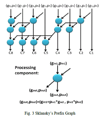
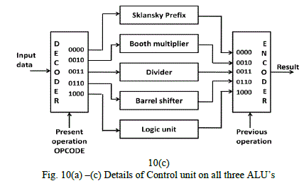
| ALU3 (low power, compact) is designed with prefix adders considered to be the most optimum amongst high speed low power adders. It uses J. Sklansky's prefix adder structure as shown in Fig 3. The delay is just log2N [4]. Hence it is faster and also less complex in hardware in comparison to CLA's. |
 |
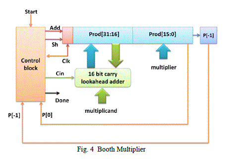
| Multiplication is implemented using the Booth multiplier shown in Fig 4[5]. This is slow compared to other multipliers and a sequential design in itself. Since 16 clock edges are required for one multiplication operation to complete, a different clock in verilog module is used which is 20 times faster than the system clock. This is accomplished using #time delay statements. Since it is based on iterative algorithm, very less hardware is used. Practically, a PLL can be used for clocking. |
 |
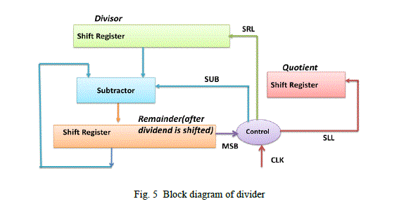
| The Divider design is based on iterative subtraction (shift &subtract). The block diagram of such a divider is shown in Fig 5. The divider used in this work is a 16-bit by 8-bit divider [6]. |
 |
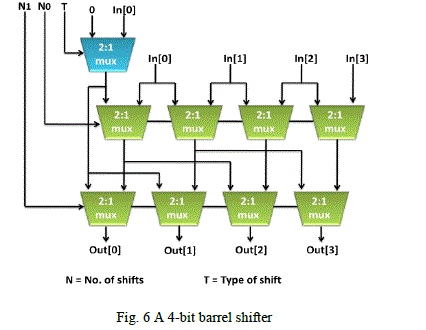
| Shift and rotate operations are taken care of by Barrel shifter built using 2:1multiplexer as shown in Fig 6. This is one of the fastest and the simplest way of doing it. |
 |
| Logical unit is not taken as a separate module but statements and built-in functions of verilog are made use of. Altogether 8 logical operations can be done, with bit-reset being a special one. In order to facilitate full-fledged processor operation, memory is a must. A dual port SRAM is modelled in verilog to hold data for processing and a ROM like memory is also inculcated for storing the instruction set. The opcodes are stored in these and fetched during operation. The status/flag register is a hardware register which contains information about the state of the processor. This design makes use of carry/borrow, negative, overflow, parity and zero flags as shown in Fig 7. |
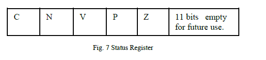 |
| Individual bits of the status register are implicitly or explicitly read and/or written by the machine code instructions executing on the processor. |
III. DESIGN OF RISC PROCESSOR |
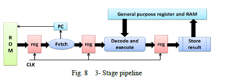
| Attempts to achieve scalar and better performance have resulted in a variety of design methodologies that cause the CPU to behave less linearly and more in parallel. One of the simplest methods used to accomplish increased parallelism is to begin the first steps of instruction fetching and decoding before the prior instruction finishes executing. This simple technique known as instruction pipelining is utilized in almost all modern general-purpose CPUs [7]. Fig 8 shows the 3-stage pipeline structure used in this work. |
 |
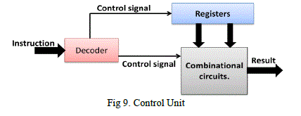
| The control unit (CU) coordinates the components of a computer system. It directs the operation of the other units by providing timing and control signals. All computer resources are managed by the CU. The control unit is a finite state machine that takes as its inputs the Instruction Register, the status register (which is partly filled by the status output from the ALU), and the current major state of the cycle. In the current design different combinatorial blocks like adders, multipliers, logic or shifters are selected depending on opcodes by control logic as shown in Fig 9. The corresponding registers from which data is to be fetched is also selected by CU. |
 |
| Fig 10 illustrates the details of the control unit which includes decoding the instruction and encoding the results on all three models[8][9]. |
 |
 |
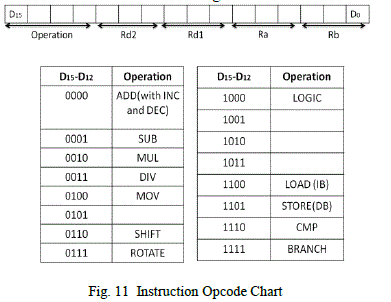
| The opcodes that are designed have the structure as shown in Fig 11. |
 |
| The opcodes that are designed have the structure as shown in Fig 11. |
 |
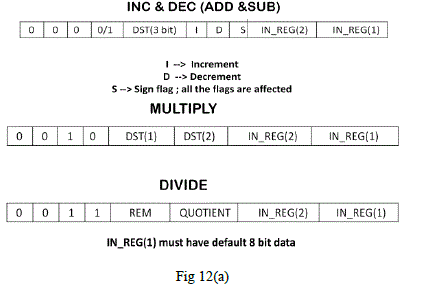
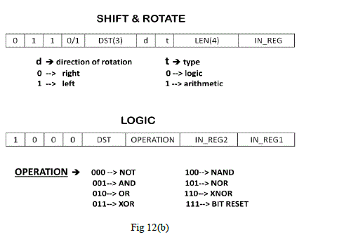
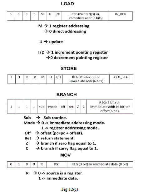
| A set of 8 general purpose registers from R0 to R7 have been used to aid in program execution. The assembled instructions are stored in memory. The detailed description of the instruction set designed is shown in Fig. 12. |
 |
 |
 |
| Since there are 8 registers, 3 bits of opcode are sufficient to address them. Since arithmetic operations need two input registers and one or two destination registers, 12 bits are set aside for the same. Wherever they aren‘t needed, special bits have been introduced. |
| Since registers are 16 bit long, Len (4) indicates the number of bits to shift or rotate. |
| Fig. 12 (a)-(c) Detailed Instruction Set |
| Branch instructions usually break the pipeline when control is taken away from usual course of instructions. To avoid this from happening, we have used yet another novel approach. We make use of the programming in Verilog to emulate a hardware which acts upon branch instructions separately, on finding them in the fetch stage. Thus further instructions are not fetched and latency or breakage is avoided. |
| As seen from the flow-chart in Fig 13, on finding the branch instruction in the fetch stage, further fetching is stopped and based on the opcode of branch instruction suitable actions are performed. |
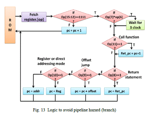 |
| For instance, when the Offset mode bit is set, then PC is given that offset to jump to or if the instruction is of Return from subroutine type, then PC value is suitably changed. When branching is based on flags like carry and zero, then process is halted for 2 clock cycles so that the previous instruction can complete execution and corresponding flags updated. This structure is highly efficient in signal processing applications as lots of branch instructions are present. |
IV. CONVOLUTION PROGRAM IMPLEMENTATION |
| The ALU is the core in DSP and ASIC where it is used in comparison, convolution, correlation, and digital filters. An ALU combines a variety of arithmetic and logic operations into a single unit. After designing an ALU, the necessity to verify and validate its performance is as such mandatory. DSP processors basically strive on filtering applications that need linear or circular convolution to be performed on inputs. As such these are RISC designs and hence we intend to implement Circular convolution on our processor . |
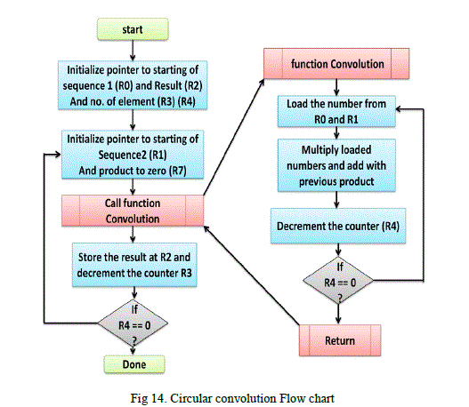 |
| Fig.14 illustrates the algorithm used for convolution. |
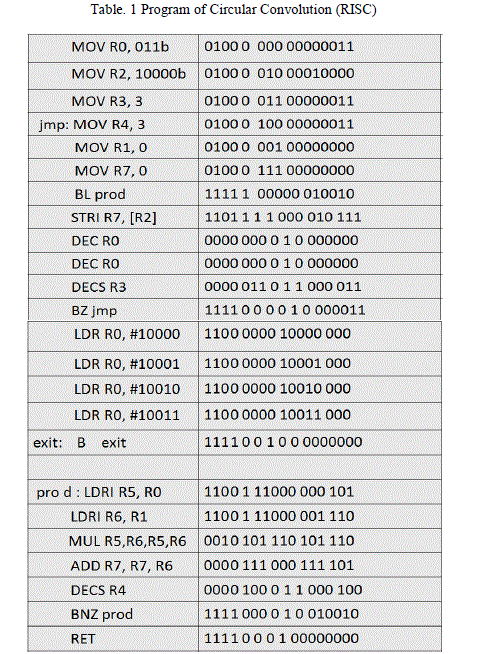 |
| Based on the algorithm, a RISC assembly program is written as shown in Table 1. The opcodes stored in the ROM, are fetched during execution. This program convolves any two sequences of 3 numbers. |
V. FPGA IMPLEMENTATION AND RESULTS |
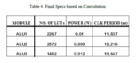
| The designs are implemented in Verilog HDL. For simulation and synthesis, Xilinx-ISE tool is used. Target device is SPARTAN-6 FPGA, based on 45 nm technology. In this project we use target technology and perform place& route operation for system verification. The inbuilt Timing Analyzer is utilized for speed based comparisons; X-power analyzer takes care of power analysis. Area of a design on FPGA is in terms of number of LUT‘s which is obtained from design summary. |
 |
| Table. 3 Comparison of Multipliers |
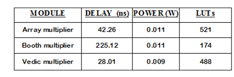 |
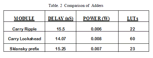
| Table 2 illustrates the comparison of specs of Adders designed, confirming high speed of CLA‘s. Table 3 illustrates comparison of specs on multipliers with booth occupying minimal area and Vedic being fastest. The specs of the other blocks are given below: Divider: The design has 125 LUTs, consumes 0.01W of power and delay of 112.6ns. Barrel Shifter: The design has 68 LUTs, consumes 0.004W of power and delay of 11.4ns. Dual Port RAM: Our design has just 32 words of memory, each 16 bit wide. The synthesized RTL has 512 registers and utilized 41 IOBs. ROM: Our design had just 32 words of memory, each 16 bit wide. The synthesized RTL uses 8 LUT‘s and 22 IOBs. |
 |
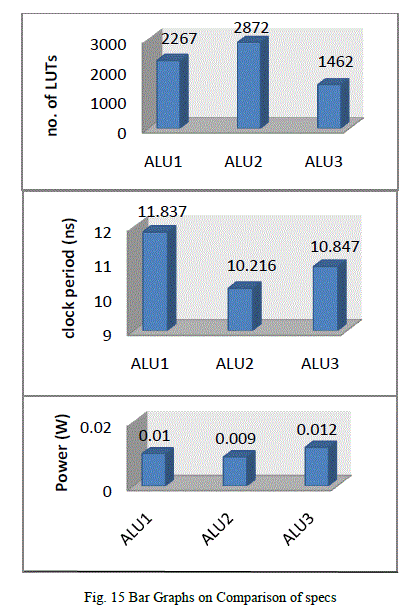 |
| The bar graphs of Fig 15 show a comparison of specs on the 3 ALU‘s. |
VI. CONCLUSION AND SCOPE FOR FUTURE WORK |
| ALU1 is built in a simplistic way without tendering to power or delay or area constraints. Such structures are best made use in modules where performance in itself is not a priority but accuracy, pricing are. Low priced computing products, low cost controllers etc use them. ALU2 (Vedic) is a generic high end product which caters to modern day demands of high speed, low power consumption and moderate area occupancy. Parallelism is best made use in these structures which has Carry- Lookahead adder and Vedic multiplier. High speed processors, mobile application processors and signal processing based devices (scopes), desktop PC‘s etc use them. ALU3 is a tricky design. The focus here is to reduce area of the architecture compromising in both speed and power. Chip size is also a major concern in modern day designs since products scale down in size. Many applications desire such products where either of the three constraints has a higher preference over others. Sensor based applications are the best examples for these which serve for military and other purposes. Thus we see how different structures are combined and varied spec results obtained. The combinations can be changed for sure, to obtain better results. For example prefix adders can be used as building blocks of multipliers which when used in the Vedic multiplier becomes a high speed and low power design which also tenders to minimal area requirements. Going ahead, use of more complex prefix adders like Kogge-Stone adder can boost the performance. Also dividers based on algorithms like Newton Raphson, rather than sequential, can be utilized to achieve higher speed of execution. The next major step continuing the work would be to design a compiler for the processor and implement the design on a PCB. This would definitely require software expertise and also knowledge of the circuit design process. |
References |
|