International Journal of Innovative Research in Science, Engineering and Technology
ISSN ONLINE(2319-8753)PRINT(2347-6710)
ISSN ONLINE(2319-8753)PRINT(2347-6710)
Rajini K. R.1, Shubha G. N.2
|
| Related article at Pubmed, Scholar Google |
Visit for more related articles at International Journal of Innovative Research in Science, Engineering and Technology
Digitally controlled pulse width modulator have gained increased attention because of a number of potential advantages including lower sensitivity to parameter variations, programmability, reduction or elimination of external passive components, as well as possibilities to implement more advanced control, calibration, or protection algorithms. This paper describes a design and implementation of runtime reconfigurable high-resolution digital pulse width modulator on low-cost general-purpose field-programmable gate arrays (FPGAs) without any manual placement and routing effort. This implementation does not depending on specialized phase locked loop (PLL) or high performance digital clock managers (DCM) which are presents exclusively in high-end vertex-6 FPGA. This implementation based on internal carry chains and logic resources, which are presents in most FPGA families. The proposed DPWM combines a counter based approach with a tapped delay line scheme for increased resolution without unnecessarily increasing the clock frequency. The experimental results show an implementation in a low-cost FPGA (Xilinx Spartan-3) that uses a 1 MHz clock frequency for a final time resolution under 1ps.
Keywords |
| pulse width modulation, tapped delay line, field programmable gate arrays, hybrid circuits, carry chains. |
INTRODUCTION |
| Digital pulse width modulator (DPWM) is an important part of digital switching power controller. It converts the digital duty ratio into PWM wave. High resolution DPWM is required to avoid limit-cycle oscillation in digital SMPS. Many architectures are proposed since 1997, such as delay line, sigma-delta and hysteretic modules, etc. Sigma-delta type can achieve high resolution without high bits of DPWM, but suffers from the problem of poor transient response. Hysteretic module is easy to implement and can reach high resolution, however its switching frequency is not constant. Delay line types are popular for its simplicity. Hybrid DPWM can achieve high resolution without taking very large die size. |
| The high performance tapped delay line based Pulse width modulators are required by the field programmable gate array based digitally controlled power converters to achieve the high efficiency at low voltage [1]. In order to optimize circuit resources in terms of occupied area and power consumption, a general architecture based on tapped delay lines is proposed, which includes segmentation of the input digital code to drive binary weighted delay cells and thermometerdecoded unary delay cells [2]. While most of the features required from the DPWM can be obtained with conventional digital design procedures, achieving fine time resolution to meet the required voltage regulation accuracy and to avoid undesired limit cycling [3], [4] is still a challenge. |
| Many approaches have been proposed in recent years to address this issue. Within FPGA implementations of hybrid DPWMs, two different approaches have been pursued. The first one takes advantage of embedded resources present in modern FPGAs, such as phase-locked loops (PLLs) or digital clock managers (DCM), to perform the delay-line functionality. A DCM-based DPWM with 2.5-ns resolution was proposed in [5], but it requires a considerable amount of additional logic and manual placement effort. A similar approach in [6] achieved under 20-ps resolution, which is the highest resolution reported to date. However, it requires a high performance DCM that may not be present in generalpurpose FPGAs, and it also relies on the update time of the DCM phase-shift command, thus limiting its applicability. Recent work in [7] has claimed that resolutions as high as 56 ps are achievable with specialized I/O delay buffers, but such elements are present exclusively in high-end Virtex-6 FPGAs. |
| The second family of solutions makes use of standard internal logic elements/blocks of the FPGA to construct the delay line [8], [9]. This approach removes the need for specialized PLL or DCM resources, but requires more complex implementations that depend on manual placement and routing, and the resolution is limited by propagation delays of FPGA logic elements/ blocks. Carry-chain logic paths are often used to implement the delay-line functionality due to their low latency and presence in most FPGAs [10]–[13]. This approach was used to construct a DPWM with 70–80 ps resolution in [14] without the need for a multiplexer. However, such an approach still requires significant manual placement effort, which, if not done properly, may lead to nonmonotonic operation or other timing errors. |
II. CLASSIFICATION OF DIGITAL PULSE WIDTH MODULATORS |
| In digital world for the implementation of pulse width modulator, it uses two methods to generate the PWM signals one is “Tapped delay-line scheme” another one is “Counter-comparator method”. Both have some disadvantages like requires more area and consumes more power respectively. To overcome those disadvantages this paper proposing a new model called hybrid delay- line /counter architecture, this combines both the properties of the tapped delay line approach and counter comparator method. |
A. Counter Comparator Scheme |
| When using analog circuits, a PWM signal is typically created by comparing a ramp signal to a reference Value with a static comparator (a static comparator is one, which requires DC current draw). Digital PWM circuits can avoid the problem of static power dissipation. A previously reported method of creating a PWM signal from a digital command is to use fast-clocked counters, but the pourer of the reported controller alone is approximately milli watts. A clock frequency fclk is chosen to be 2N times the switching frequency, fsw, where N is the number of bits in the digital command word. The clock is used to divide the switching period into 2N increments. This method requires the use of very fast clocks for large values of N, and the need to run an N bit counter at fclk precludes the use of low supply voltages, which would otherwise save power. Fig.1 shows the fast-counter digital PWM generation scheme. |
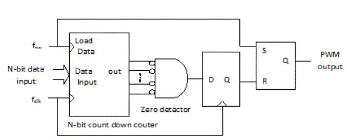 |
B. Tapped Delay Line Scheme |
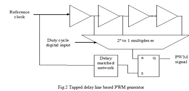
| Another way to create a pulse width modulated signal from an N-bit digital value is to use a tapped delay line. Since this approach uses the switching frequency clock, the power is significantly reduced relative to the fast-clocked counter approach. Fig. 2 shows a schematic for the proposed digital word-to-PWM circuit. The essential components of a tapped delay line PWM circuit are the delay line and a multiplexer. A pulse from a reference clock starts a cycle, and sets the PWM output to go high (after a delay designed to match the propagation delay experienced through the multiplexer). The reference pulse propagates down the delay line, and when it reaches the output selected by the multiplexer, it is used to set the PWM output low. The total delay of the delay line is adjusted so that the total delay is equal to the reference clock period. That is, feedback is used to turn the delay line into a delay-locked-loop (DLL), which locks to the period of the input clock. Multiple PWM signals can be generated by adding multiplexers to a single delay line, a feature that might be used to create a timing signal to turn off a synchronous rectifier. |
 |
C. Hybrid DPWM Architecture |
| Fig.3 is one of the most widely used architectures. It combines reliable, synchronous modulation techniques to achieve coarse (clock frequency) resolution, with a delay-line-based approach that provides high resolution without the need for a very high frequency clock. The delay-line section usually contains tapped delay elements and a multiplexer to control the amount of delay applied to the input signal. |
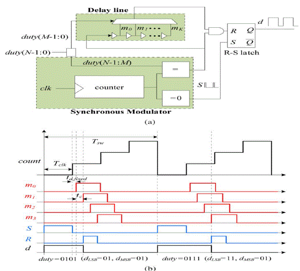 |
| In the N-bit hybrid DPWM shown in Fig.3, the output signal d is set high by the counter at the beginning of the switching period, and is reset by the delay-line output within the desired clock period selected by the most significant bits (MSB) of the duty cycle, dMSB = duty(N − 1 : M). The system clock is usually taken as the input signal to the delay line, and delayed by an amount controlled through a multiplexer, using the least significant bits (LSB) of the duty cycle command, dLSB = duty(M − 1 : 0). Therefore, synchronous logic handles the MSB part of the duty cycle command, whereas an asynchronous section (tapped delay line and multiplexer) resets the duty cycle signal and determines the resolution. Careful routing and placement are required to match the delay of the critical signal paths; the 2M tapped delay-line outputs that go through the multiplexer must be delay-matched within at least one unit delay. Failure to do so causes nonmonotonicity a malfunctioning of the DPWM. |
III. HYBRID DPWM ARCHITECTURE |
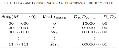
| Fig. 4 shows a simplified delay line based on carry-chain logic as proposed in [14]. The carry chain is a low latency path, which is used to propagate the carry bit through consecutive 2-bit adders to implement high-speed arithmetic operations. When Di goes high, logic 1 propagates through the carry chain. Rather than tapping and multiplexing each delay element output, the control word D is used to select the position of the chain where the carry begins to propagate. The propagation delay tc of the carry bit through each adder is fixed and predictable, and usually lays in the range of 10–100 ps, depending on the FPGA. This propagation delay sets the minimum achievable time resolution of the DPWM. The digital word duty (M − 1 : 0) = dM−1dM−2 . . . d0 ∈ [0, 2M −1 = K] determines the total delay, tdelay , of the carry chain, in the following manner: |
| tdelay = td,fixed + duty ãÃÆû tc (1) |
| with td,fixed being the propagation delay from the output of the decoder to the actual input of the carry-chain element where the propagation begins. From (1) and Fig. 2, it can be seen that 2M delay elements are required to implement a Mbit delay line. Furthermore, note that an ideal hybrid DPWM should fulfil |
| Tclk = td,fixed + K ãÃÆû tc (2) |
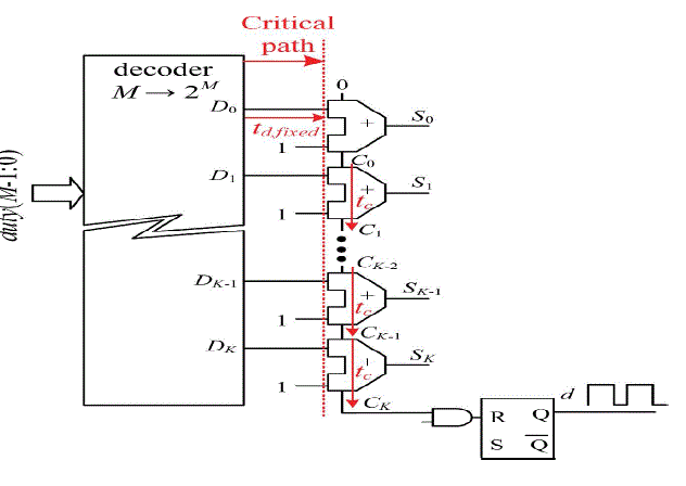 |
| with Tclk being the system clock period. Table I shows the value of the digital word D and the desired delay as a function of the duty cycle command. Note that tc remains approximately constant among different elements and thus, according to (1), linearity and monotonicity are mainly determined by the delay through the critical path, td,fixed. Given the low value of tc that the carry-chain logic provides, an almost perfect match between the routing delay from each output of the decoder Di to the input of each corresponding adder is required to achieve a monotonic, repeatable, and reliable behaviour. This means that, although the carry chain is automatically placed by the FPGA programming tools, the decoding logic still requires very careful manual placement and routing, significantly increasing complexity, and development time. The next section presents the main contribution of this letter, two simple implementation approaches that guarantee the required delay matching without the need for manual placement and/or routing. |
 |
IV. DPWM IMPLEMENTATION |
| According to Fig.4, there are at least 2M signals in the critical path that need to be matched within a few picoseconds. This section describes two different implementations that target the most widely used FPGA families, which achieve high-timing resolution and maintain simplicity of implementation without manual placement or routing effort by leveraging the inherent, default routing optimization routines of associated development tools. |
A. Implementation in Xilinx FPGAs |
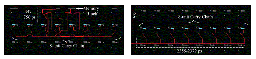
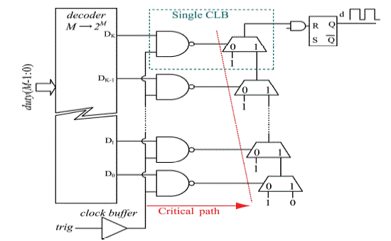
| Embedded memory blocks are available in Xilinx devices. The Xilinx Spartan-3 and associated auto routing tools do not natively match the routing delay of each output from the RAM block. Fig.5 is used to remove the routing from the decoder to the carry chain as a critical circuit path. In Figure 5, the multiplexer devices responsible for implementing the fast carry-chain path are shown explicitly as the delay elements, and an NAND gate is used to control their selection input so that propagation through the carry chain is only allowed to begin when the trig signal goes high. By gating the output of the decoder thusly, the path from decoder to NAND gate is no longer critical to be delay matched; instead, only the delay of the trig signal through each NAND is critical. This implementation is similar to that presented previously in [14], where the reduced matching requirements allowed near-monotonic operation, with full monotonicity obtained with a small-manual placement effort. However, inherent Xilinx routing routines can be used to ensure optimal placement natively by instantiating devices from primitives directly, eliminating the need for any manual placement or routing. To accomplish this, the internal structure of each Xilinx spatan-3 configurable logic block (CLB) is examined. As is the case with most FPGAs, the select pins of carry-chain multiplexers implemented within each CLB are directly wired to the output of a look up table (LUT). Because the NAND function can be implemented in this LUT, internal to the same CLB as the multiplexer, the delay from NAND output to multiplexer can be extremely well matched between CLBs and thus between delay elements. In order to ensure such matching, the lock_pins constraint is used on each LUT to maintain identical signal paths from trig to each delay element. Finally, to ensure that the trig signal itself is delay matched to each NAND, a clock buffer primitive is used to give the signal access to low-skew routing paths, the result of which can be seen in Fig.5(b), which show less than 17 ps propagation mismatch of the trig signal to the 16 NAND gates, according to the delays calculated by the Xilinx tools. |
 |
| Default routing routines inherent to the Xilinx development tools for the Spartan-3 natively maintain the structure of the carry chain for optimal timing, so no manual placement or routing is necessary. Furthermore, directly from primitives, instantiating carry-chain multiplexers and NAND gates (LUT2) automatically combine the LUT elements into the same CLB as the carry chain they control. |
 |
V. EXPERIMENTS |
| The architecture was implemented in Xilinx Spartan-3 FPGA and version 13.2 of the Xilinx ISE design suite. |
 |
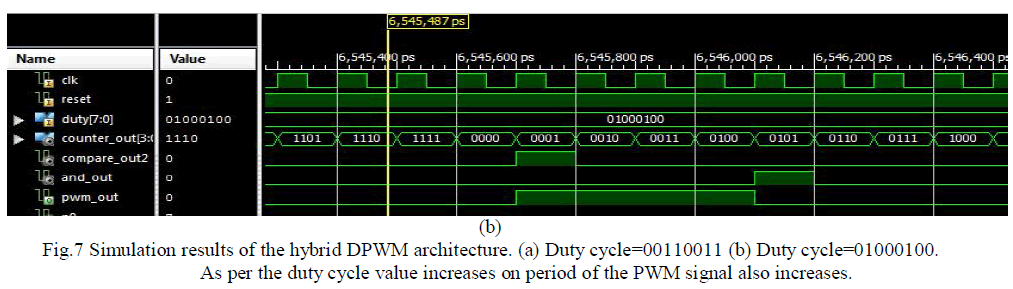 |
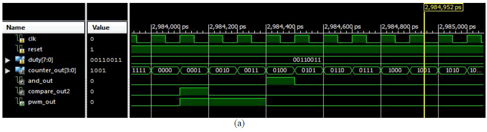
| Duty cycle is the main input in DPWM and it is stored in terms of binary numbers (N-1:0). LSB (M-1:0) are used to implement the duty cycle and MSB(N-1:M) are used for synchronous modulator. Figure 7 (a) and (b) show the PWM signal for 8 bits duty cycle and 8 bits are equally divided in to 4 bits LSB and 4 bit MSB. S-R flip flop is used to set and reset the output value depending on input duty cycle here we can control the ON time and OFF time of the PWM signal. |
VI. CONCLUSION |
| This paper has demonstrated a very simple, design and implementation of runtime reconfigurable high resolution digital pulse width modulator architecture using general purpose low cost field programmable gate array(FPGA) without any manual placement and routing efforts.. The proposed architecture achieves very high resolution using the propagation delay through internal carry chains normally used to perform high-speed arithmetic operations. This approach provides a excellent linearity, reliability, low latency, low variability delay line that is automatically instantiated by the compiling tools. This fact, in conjunction with further use of specific internal FPGA resources that provide matched routing delay to the input of the delay chains.The proposed approach has been demonstrated through a 1-MHz switching frequency, 8-bit, 1 ps time resolution DPWM without manual placement and routing. |
References |
|