this paper presents the use of a stepupdc-dc converter by cascading cock croftwalton voltage multiplier for a hybrid system. The hybrid renewable energy system used is a combination of as olar panel and a fuel cell. the conventional method isto use a converter increase the voltage and further uses a transformer to increase the voltage level of the output. The p ro p o s ed converter topology used is boost converter cascaded with an n-stage cockcroft-walton voltage multiplier. the number of stages of the voltage multiplier increases the output level of the stepupdc-dcconverter which drives the load. The converter-voltage multiplier module provides continuous conduction with the voltage stress on cascaded capacitor-diode and switches being reduced. The output voltage obtained can be used in highvoltage applications .the simulation of the entire topology for hybrid system was done using matlab software.
Keywords |
| Cockcroft-Walton (CW) voltage
multiplier, solar panel, fuel cell, step-up DC-DC
converter. |
INTRODUCTION |
| In the present scenario throughout the world, everyone is
concerned with fossil fuel exhaustion and environmental
problems caused by conventional power generation.
Hence renewable energy sources are used among which
solar panels and wind generators are the most used. The
solar panel generally uses a power converter for
connecting with the load. The efficiency of photovoltaic
(PV) module is too low and output power depends on
insolation level and temperature. Therefore the solar or
PV panel is used along with a fuel cell (FC) system
making it a hybrid renewable energy system. The hybrid renewable energy system is a combination of two or
more renewable energy system to obtain higher
efficiency than from a single energy power source. The
fuel cell used converts an oxidant and fuel into electricity
through an electrochemical process. They produce very
low emissions and have high operating efficiencies. The
converter topology used is a step-up converter which is
cascaded with a Cockcroft-Walton (CW) voltage
multiplier which increases the voltage level. |
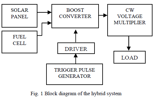
II. HYBRID SOLAR PANEL/FUEL CELL SYSTEM |
| The block diagram of the hybrid solar and fuel cell
system with the power converter is show in the Fig. 1. It
consists of solar panel, a fuel cell, a boost converter
topology, CW voltage multiplier, a pulse generator and
load. The solar panel is used as the primary supply and
fuel cell as the backup supply. The converter is used to
boost up the input voltage from the hybrid solar
panel/fuel cell system. |
 |
| A.Solar Panel |
| The solar panel is a linked collection of PV modules,
which is in turn made of multiple interconnected solar
cells. The cells convert solar energy into electricity by
photovoltaic effect. The power one PV module produces
is enough to power a residential place. The collection of
solar panels is a solar array. The solar array generally
requiresan inverter to convert DC power to AC powerso it
can be used to supply AC loads. The modules of the solar
panel are connected in series to obtain the required
voltage and the individual strings are connected in
parallelto increase the current. The photons in sunlight
thatstrikes the panel are absorbed by semiconducting
materials like silicon. The electrons present in the
semiconductor material are knocked out from the atoms
that cause an electric potential difference. Thus current
starts to flow through the silicon to eliminate the potential
and hence electricity is captured which is then supplied to
the load. The equivalent circuit of solar cell is shown
below as in Fig. 2. |
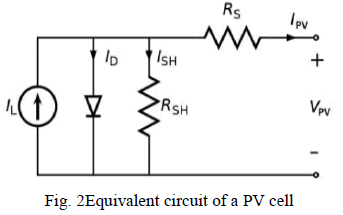 |
| Applying KCL to equivalent circuit, |
 |
| Applying KVL to equivalent circuit, |
| VPVcell = VD - RSIPV(2) |
| The PN-junction diode characteristics is given by, |
 |
| B. Fuel Cell |
| The fuel cell used is a Proton Exchange Membrane (PEM)
fuel cell that consists of an electrolyte which is a small,
thin, and light permeable polymeric membrane. The
reaction is catalysed using platinum electrodes are used on
both sides of the membrane. The hydrogen molecules are
supplied at the anode which splits the molecules into
electrons and hydrogen protons. The protons pass through
the polymeric membrane to the cathode while the
electrons are passed round an external circuit to produce
electricity. Oxygen is supplied to the cathode which
combines with hydrogen to produce water.Hydrogen
molecules are supplied to fuel cell directly or from natural
gas, methanol or petroleum. Each electrode assembly has
two electrodes of anode and cathode with a layer of
catalyst which is thin. The desired amount of electrical
power can be obtained by combining individual fuel cells to form a fuel cell stack. The output voltage of a single
fuel cell is given by the equation, |
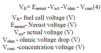 |
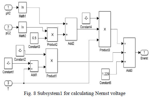
| The Nernst voltage of the fuel cell is, |
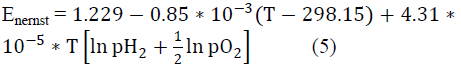 |
| T - temperature (K) |
| pH2 - partial pressure of the Hydrogen (atm) |
| pO2 - partial pressure of the oxygen (atm) |
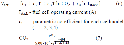
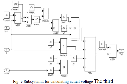
| The activation potential having anode & cathode is given
by, |
 |
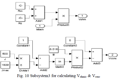
| The ohmic voltage drop or loss is provided by the
following equation, |
 |
| Rm - resistance to transfer of protons through
membrane |
| Rc- resistance of the membrane to electron flow |
| The voltage drop due to mass transport or the
concentration voltage is given as |
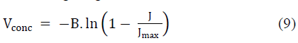 |
| B - parametric coefficient depending on the fuel
cell |
| J - actual current density of the fuel cell (A/m2) |
| Jmax- maximum current density of the fuel
Cell (A/m2) |
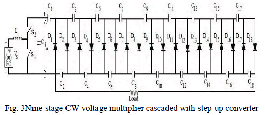
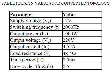
III. CONVERTER TOPOLOGY FOR HYBRID
SYSTEM |
| The converter circuit consists of the step–up converter
topology by which two switches are connected in series
having an inductor in between the two switches. The
converter also has a capacitor connected in parallel to the
switches. The converter circuit output is then given to a
CW voltage multiplier which is made of n-stages. The
CW voltage multiplier converts AC or DC voltage from a
lower level to a higher DC level. The output voltage of
CW voltage multiplier depends on the number of stages and voltage across the even capacitors. The advantage is
that it is easy to insulate, requires low cost components
and the voltage gain is proportional to the number of
cascaded stages. It also utilises the output from any stage.
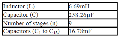
The converter topology consists of nine stages. Hence
there are 18 capacitors and 18 diodes. Each stage consists
of two diodes and two capacitors respectively.The
relationship between the supply voltage of the converter
and capacitor voltage of CW voltage multiplier converter
is given by |
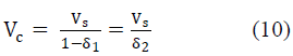 |
| The change in inductor current and capacitor voltage of
converter are given by |
 |
| The inductance (L) and capacitor(C) of the converter are
given by |
 |
| The time period of the converter is given as |
 |
 |
| The output voltage and output current of CW voltage
multiplier are given as |
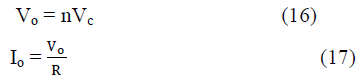 |
| The change in capacitor voltage of CW voltage multiplier
is given by |
 |
| The capacitor of the CW voltage multiplier is given by |
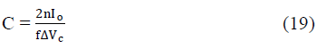 |
| A. Operating Principle |
| Theoperating principle of the converter topology
depends on the terminal current ia which is a pulsating
form current. The switches are given gate pulse by trigger pulse generator through a drive circuit. The modes of
operation are as follows: |
| Mode-I: S1 and S2 are turned OFF and diodes (D1 to D18)
do not conduct.The inductoris charged by input DC from
the hybrid system, hence the odd numbered capacitors
(C1,C3,C5,C7,C9,C11,C13, C15andC17) float while even
numbered |
| Capacitors (C2, C4, C6, C8, C10,C12, C14, C16 and C18)
supply the load. |
| S1 and S2 are turned ON and the current ia is positive for
modes II to X. The inductor is discharged and input
source transfers energy to the CW voltage multiplier
through the even numbered diodes. |
| Mode-II: D18isturned ON, at the same time the other
diode do not conduct hence C2, C4, C6, C8,C10, C12, C14,
C16 and C18gets charged whileC1,C3,C5,C7,C9,C11, C13,
C15 and C17are all discharged byia. |
| Mode-III:D16 is turned ON hence C2, C4, C6, C8,C10, C12,
C14 and C16gets charged while C1,C3,C5,C7,C9,C11, C13
and C15 are discharged byia.Hence C18 supplies the load
while C17 floats. |
| Mode-IV:D14 is turned ON hence C2, C4, C6, C8,C10, C12
and C14 gets charged while C1,C3,C5,C7,C9,C11 and C13
are discharged byia. Hence C16 and C18 supply the load
while C15 and C17 floats. |
| Mode-V: D12 is turned ON hence C2, C4, C6, C8,C10 and
C12 gets charged while C1,C3,C5,C7,C9 and C11 are
discharged by ia. Hence C14, C16 and C18 supply the load
while C13, C15 and C17 float. |
| Mode-VI: D10 is turned ON hence C2, C4, C6, C8 and C10
gets charged while C1,C3,C5,C7 and C9 are discharged by
ia.Hence C12, C14, C16 and C18 supply the load while C11,
C13, C15 and C17float. |
| Mode-VII:D8 is turned ON hence C2, C4, C6 and C8 gets
charged while C1,C3,C5 and C7 are discharged by ia.
Hence C10, C12, C14, C16 and C18 supply the load whileC9,
C11, C13, C15and C17 float. |
| Mode-VIII: D6 is turned ON hence C2, C4 andC6 gets
charged while C1,C3 andC5 are discharged by ia. Hence
C8, C10, C12, C14, C16 and C18 supply the load while C7,
C9, C11, C13, C15 and C17 float. |
| Mode-IX:D4 is turned ON hence C2 and C4 gets charged
while C1and C3 are discharged by ia .Hence C6, C8, C10,
C12, C14, C16 and C18supply the load while C5, C7, C9,
C11, C13, C15and C17float. |
| Mode-X:D2 is turned ON hence C2 gets charged while C1
is discharged by ia. Hence C4, C6, C8, C10, C12, C14, C16
and C18supply the load whileC3, C5, C7, C9, C11, C13, C15
and C17floats. |
| S1 and S2 are turned ON and the current ia is negative for
modes XI to XIX. The inductor is discharged and input
source transfers energy to the CW voltage multiplier
through the odd numbered diodes. |
| Mode-XI:D17 is turned ON while diodes (D1to D16and
D18) do not conduct hence C2, C4, C6, C8,C10, C12, C14 and
C16 are all discharged whileC1,C3,C5,C7,C9,C11, C13, C15
and C17 are all charged by ia. Hence C18 supplies the load.
Mode-XII: D15is turned ON hence C2, C4, C6, C8,C10, C12
and C14are all discharged while C1,C3,C5,C7,C9,C11, C13
and C15 are charged by ia. Hence C16 and C18supply the
load while C17 floats. |
| Mode-XIII:D13is turned ON hence C2, C4, C6, C8,C10 and
C12gets discharged while C1,C3,C5,C7,C9,C11 and C13are
all charged by ia. Hence C14, C16 and C18supply the load
while C15 and C17floats. |
| Mode-XIV:D11 is turned ON hence C2, C4, C6, C8and
C10are all discharged while C1,C3,C5,C7,C9 and C11are all
charged by ia. Hence C12, C14, C16 and C18supply the load
while C13, C15 and C17float. |
| Mode-XV: D9 is turned ON hence C2, C4, C6 and C8 are
discharged while C1,C3,C5,C7 and C9 are charged by ia.
Hence C10, C12, C14, C16 and C18supply the load whileC11,
C13, C15 and C17float. |
| Mode-XVI:D7is turned ON hence C2, C4 and C6are all
discharged while C1,C3,C5 and C7 are charged by ia.
Hence C8, C10, C12, C14, C16 and C18supply the load
whileC9, C11, C13, C15 and C17 float. |
| Mode-XVII:D5is turned ON hence C2 and C4 gets
discharged while C1,C3 and C5 are charged by ia. Hence
C6, C8, C10, C12, C14, C16 and C18supply the load while C7,
C9, C11, C13, C15 and C17float. |
| Mode-XVIII:D3 is turned ON hence C2 is discharged
whileC1 and C3 are charged b yia. Hence C4, C6, C8, C10,
C12, C14, C16 and C18supply the load whileC5, C7, C9, C11,
C13, C15 and C17 are floating. |
| Mode-XIX:D1 is turned ON hence C1 is charged by ia.
Hence all even capacitors supply the load while C3, C5,
C7, C9, C11, C13, C15 and C17float. |
 |
 |
IV.SIMULATED CONVERTER TOPOLOGY FOR
HYBRID SYSTEM |
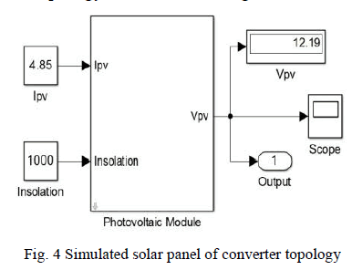
| The simulation of the converter for the hybrid system is
done using MATLAB software. The solar panel is used
as the primary supply. The simulated solar panel of
converter topology is shown as in Fig. 4. |
 |
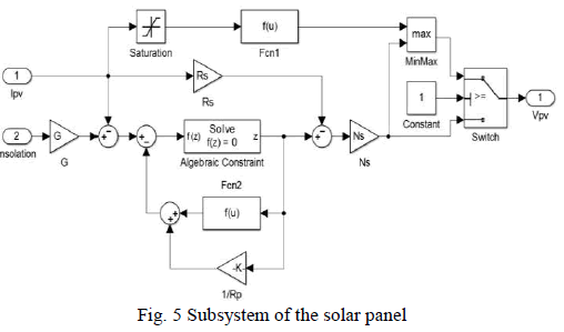
| The solar panel has a subsystem which contains the
design equations based on the equivalent circuit of a solar
cell. |
 |
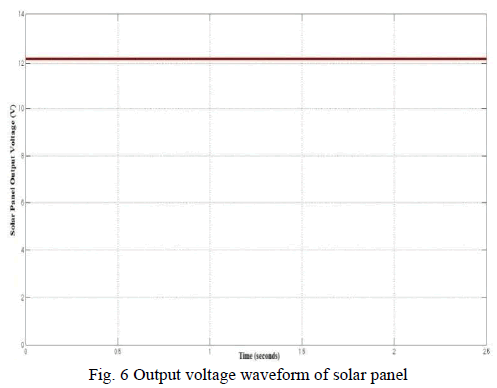
| The output waveforms and results obtained can be used
so that it is easier to design the prototype model. The
waveform of the output voltage of solar panel is shown
below in Fig.6. |
 |
| The fuel cell is used as a back-up to the solar panel. The
fuel cell and the solar panel are connected in parallel.
Therefore only one will be used at a time. The simulated
fuel cell is shown |
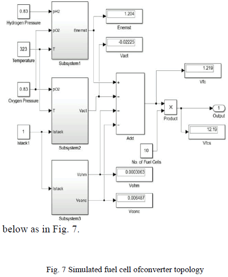 |
| The first subsystem is the calculation of the Nernst
voltage (Enernst). The simulated subsystem1 for calculating
the Nernst voltage is shown in Fig. 8. |
 |
| The second subsystem of the fuel cell is calculation of the
actual voltage (Vact). The simulated subsystem for
calculating the actual voltage is shown in Fig. 9. |
 |
| subsystem of the fuel cell is for calculating the ohmic
voltage drop (Vohmic) and the concentration voltage
(Vconc). The simulated subsystem is shown as in Fig. 10. |
 |
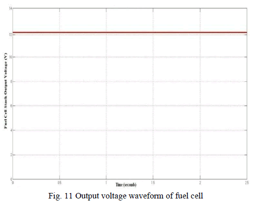
| The simulated fuel cell has one output waveform which
is the output voltage shown as in Fig.11. |
 |
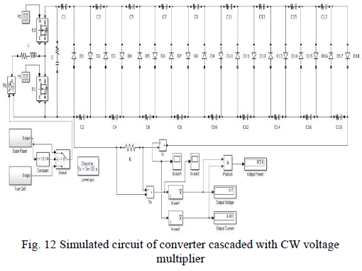
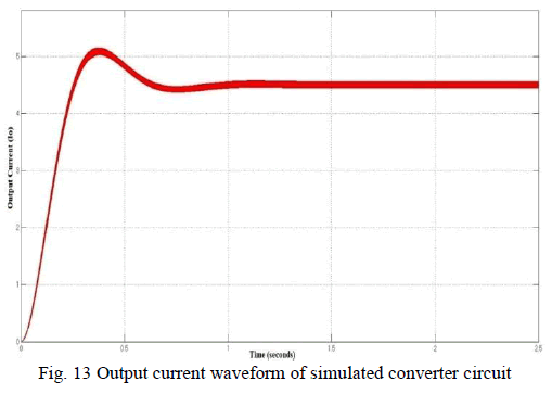
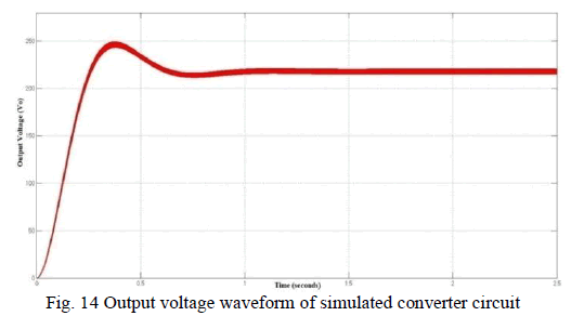
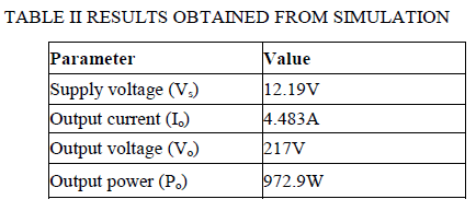
| The simulated circuit consists of two output waveforms of
the output voltage and output current.From the waveforms
it can be observed that after a certain point the steady state
is achieved.The simulated converter for the hybridsystem
is show in Fig. 12. |
 |
 |
 |
 |
V. CONCLUSION |
| In this paper, the solar panel and fuel cell were designed
and simulated initially using MATLAB software. The
boost converter cascaded with Cockcroft-Walton voltage
multiplier was designed and then integrated with the solar
panel and fuel cell with solar panel as the primary source
and fuel cell as the backup. Then the entire setup was
simulated using MATLAB software. From the simulation
results it was observed that, the proposed circuit for the
hybrid system is suitable for high voltage applications.
The boost converter for Cockcroft-Walton voltage
multiplier depends on the capacitance value and number
of stages of the voltage multiplier. In future work,for the
same or any number of stages of the voltage multiplier
used the voltage level can be improved by changingthe
capacitance value. |
References |
- Berkovich Y., Axelrod B. and Shenkman (2008) âÃâ¬ÃËA novel diodecapacitor voltage multiplier for increasing the voltage ofphotovoltaic cellsâÃâ¬Ã⢠Proc. IEEE COMPEL, pp. 1-5.
- Ching-Shan Leu, Hyang P.U. and Li M.H. (2011) âÃâ¬ÃËA novel dualinductor boost converter with ripple cancelation for high voltagegain applicationsâÃâ¬Ã⢠IEEE Trans. Ind. Electronics, vol. 58, no.4, pp.1268-1273.
- Ioannis C. and Tatakis E.C. (2010) âÃâ¬ÃËOptimal design of half waveCockcroft-Walton voltage multiplier with minimum totalcapacitanceâÃâ¬Ã⢠IEEE Trans. on Power Electronics, vol. 25, no. 9,pp. 2460-2468.
- Kuo-Ching Tseng, Chi-Chih Huang and Wei-Yuan Shih (2013)âÃâ¬ÃËHigh step up converter with a voltage multiplier module for aphotovoltaic systemâÃâ¬Ã⢠IEEE Trans. on Power Electronics, vol. 28,no. 6, pp. 3047-3057.
- Luo F.L. and Ye H. (2004) âÃâ¬ÃËPositive output cascade boostconvertersâÃâ¬Ã⢠Proc. Inst. Elect. Eng.âÃâ¬ÃâElect. Power Appl., vol. 151,no. 5, pp. 590-606.
- Lung-Sheng Yang, Liang T.J. and Chen J.F. (2009) âÃâ¬ÃËTransformerless DC-DC converters with high step up voltage gainâÃâ¬Ã⢠IEEETrans. on Ind. Electronics, vol. 56, no. 8, pp. 3144-3152.
- Marcos Prudente, Pfitscher L.L., Emmendoerfer G., RomaneliE.F. and Gules R. (2008) âÃâ¬ÃËVoltage multiplier cells applied to nonisolatedDC-DC converters with high static gainâÃâ¬Ã⢠IEEE Trans. OnPower Electronics, vol. 23, no. 2, pp. 871-877.
- Phatiphat Thounthong, ArkhomLuksanasakul, PoolsakKoseeyaporn and Bernard Davat (2013) âÃâ¬ÃËIntelligent model basecontrol of standalone photovoltaic/fuel cell power plant withsuper capacitor energy storageâÃâ¬Ãâ¢IEEE Trans. on SustainableEnergy, vol. 4, no. 1, pp. 240-249.
- Rong-Jong Wai, C. Y. Lin, R. Y. Duan and Y. R. Chang (2007)âÃâ¬ÃËHigh efficiency DC-DC converter with high voltage gain andreduced switch stressâÃâ¬Ã⢠IEEE Trans. on Ind. Electronics, vol. 54,no. 1, pp. 354-364.
- Sachin Jain and VivekAgarwal (2008) âÃâ¬ÃËIntegrated hybrid powersupply for distributed generation applications fed by nonconventionalenergy sourcesâÃâ¬Ã⢠IEEE Trans. on Ind. Electronics,vol. 23, no. 2, pp. 622-631.
- Tsai-Fu Wu, Lai Y.S., Hung J.C. & Chen Y.M. (2008) âÃâ¬ÃËBoostconverter with coupled inductors and buck-boost type of activeclampâÃâ¬Ã⢠IEEE Trans. on Ind. Electronics, vol. 55, no. 1, pp. 154-162.
- Wuhua Li and He X. (2011) âÃâ¬ÃËReview of non-isolated high step upDC-DC converter in photovoltaic grid connected applicationsâÃâ¬Ãâ¢IEEE Trans. on Ind. Electronics, vol. 58, no. 4, pp. 1239-1250.
|