International Journal of Innovative Research in Science, Engineering and Technology
ISSN ONLINE(2319-8753)PRINT(2347-6710)
ISSN ONLINE(2319-8753)PRINT(2347-6710)
J.Shaba1, S.Pooranachandran2
|
| Related article at Pubmed, Scholar Google |
Visit for more related articles at International Journal of Innovative Research in Science, Engineering and Technology
Recently low power Analog to Digital Converters(ADCs) have been developed for many energy constrained applications such as wireless sensor networks and bio-medical applications. Successive approximation register (SAR) ADC are good candidates for low power applications and widely used for low energy application due to its minimum analog blocks. The static linearity performance in terms of the integral nonlinearity and differential nonlinearity and the parasitic effects of the split DAC, are analyzed. A code-randomized calibration technique is done to correct the conversion nonlinearity in the conventional SAR ADC, which is verified by behavioral simulation. Here the SAR ADC is designed in such a way that the control module completely control the splitting up of modules and the speed of operation is changed using low level input bits.A dedicated multiplexer can be used to minimize the capacitor array structure.The control module controls the clock signal and determines the time at which the analog signal should enter the SAR logic.On attaining control over the time of arrival of input signals the speed of conversion can be increased and power utilisation can be minimised.
Keywords |
| Linearity analysis, linearity calibration, SARADCs, split DAC |
INTRODUCTION |
| Successive approximation registers (SAR) analog-to-digital converters (ADCs) are used as an alternative to the pipelined ADCs for battery-powered mobile applications, such as DVB-T, DVB-H and TDMB [1] which require medium speed (10 MS/s–100 MS/s) and medium-resolution (8–10 b). SAR ADCs achieve very low power consumption due to their simple structural design and operation. However, the SAR conversion relies basically on the arrangement of a capacitive DAC that subtracts the reference voltage from the input signal. The kT/C noise, capacitor mismatches, and parasitic of the split DAC[2] affect the conversion precision. For medium resolution the kT/C noise requirement is satisfied with small capacitance, while other nonidealities like parasitic and nonlinearity, whose effect depends on the structure and the switching approach of the DAC, becomes significant. SAR ADCs uses Binary weighted capacitive DAC structure. But the capacitance of the DAC array increases exponentially with the resolution, which results in larger consumption of switching energy, area, and settling time. A valuable substitute for medium resolution[3]-[5] is the split capacitive DAC. But it has the limitation that the parasitic capacitors destroy the desired binary ratio of the capacitive DAC array, thus degrading the conversion linearity. This paper analyzes the conversion nonlinearities, induced by supply noise, switching methods, and parasitic effects in SAR ADCs.The internal node parasitic in the split DAC is also analyzed,since it degrades the conversion linearity. This limitation can be fixed by a code-randomized digital calibration technique in order to improve the differential nonlinearity (DNL) and integral nonlinearity (INL). |
SAR ADC OVERVIEW |
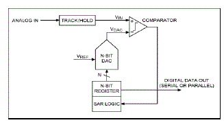
| A successive approximation ADC is a type of analog to digital converter that converts a continuous analogwaveform into a discrete digital representation via a binary search through all possible quantization levels before finally converging upon a digital output for each conversion.Successive Approximation A/D converters are one of the most popular approaches for realizing A/D converters. This is due to their advantage of having relatively quick conversion time, and moderate circuit complexity. Implementing a SAR ADC, the basic architecture is quite simple. The input voltage (VIN) is held on a track/hold. For implementing the binary search algorithm, the N-bit register is initially set to midscale (that is, 100... .00, where the MSB is set to 1). This forces the DAC output (VDAC) to be VREF/2, where VREF is the reference voltage given to the ADC. VIN is then compared with VDAC to determine if VIN is less than, or greater than, VDAC. If VIN is greater than VDAC, the comparator output is logic high, or 1, and the MSB of the N-bit register remains at 1 |
 |
EXISTING SYSTEM |
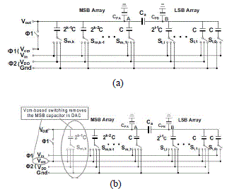
| When supply voltage is used as reference voltage the switching power becomes dynamic which is correlated with the switching sequence. Fig. 2(a) represents a conventional single-ended n-bit split DAC structure. During the global sampling phase, the input signal represented as Vin is stored in the entire capacitor array. The algorithmic conversion then starts by switching only the MSB capacitor to VDD and the others to Gnd. Accordingly, Vout settles to −Vin and the comparator output Out_{comp}in the first MSB decision will be |
 |
| The comparator output predicts the switching logic for the MSB capacitor. If Out_ {comp} results low Sm,k is switched back to Gnd. If Out_{comp}becomes high, then Sm,k maintained VDD. Simultaneously, the Sm,k−1 (the MSB/2) switches to VDDfor the next bit comparison. The above process repeats for n − 1 cycles.The conventional charge redistribution method is not effective in terms of power when discharging the MSB and charging the MSB/2 capacitor. |
| The Vcm based switching method reduces the array capacitance to half resulting in 90% energy saving when compared with conventional method.Fig.2(b) represents the Vcm based switching algorithm. During the sampling phase voltage Vin gets stored in the capacitor array. During the conversion phase the bottom-plates of the capacitors gets switched to the Vcm first, which raises the voltage −Vin at the output. |
 |
CHOICE OF THE ARCHITECTURE |
| A/D conversion is obtained with many algorithms. For obtaining power effectiveness, what often matters is not inventing new methods but finding the best use of known algorithms and achieving the optimum for the foreseen technology and the given specifications. High speed and medium-to-high resolution normally call for pipeline, two-step, or subranging schemes. The basic building blocks are the track-and-hold, the comparator, and the op-amp.With medium resolution, the input trackand- hold is a source follower with passive sampling. Clock feedthrough is minimized with dummy elements and body effect is cancelled out by connecting the source and substrate. The power depends on the capacitive load that, in turn, is proportional to the number, N, of comparators served by the T&H. Since gm/CL is the relevant parameter, the power increases with the square of N. The power of the comparator depends on the resolution. For several tens of mV, just a latch makes the comparator. For resolutions from ten to few tens of mV, however, it is necessary to use a simple preamplifier before the latch. |
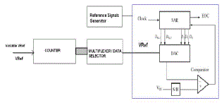
| The basic architecture of the proposed scheme is split SAR ADC with additional control module in the form of multiplexer that can control the splittg up of modules is shown in figure 3. The SAR ADC can be implemented in a configurable manner with different frequency inputs while configurable means that the entire ADC architecture can work with different performance by changing the Vref of the ADC. Normally in all ADC Vref,Vin,Vth plays a major role in ADC conversion.By varying the values of Vref we can change tyeperformance of the ADC. The different values of Vref can be stored through multiplexer. A counter can be used to select the mux inputs. Reference signal generator can be used to generate different analog signals to test the ADC structure. |
 |
ARCHITECTURE DESCRIPTION |
| A. DAC Architecture |
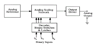
| The digital-to-analog (D/A) converter is used to decode a digital word into a discrete analog level. Depending on the application, the input signal can be voltage or current. Figure 3 shows a high level block diagram of a basic D/A converter. A binary word is stored and decoded which drives a set of switches that control a scaling network. The analog scaling network is based on voltage scaling, current scaling, or charge scaling. The scaling network is used to scale the appropriate analog level from the analog reference circuit and is applied to the output driver. A voltage scaling network is formed by a simple serial string of identical resistors between a reference voltage and ground. A switch does the work of tapping the voltages off the resistors and applies them to the output driver. Current scaling approach depends on switched scaled current sources. Charge scaling is obtained by providing capacitor divider with a reference voltage using scaled capacitors where the total capacitance value is determined by the digital code. Choice of the architecture depends on the components available in the target technology, conversion rate, and resolution. |
| In an SAR-ADC the power is mainly consumed in the DAC, the comparator, the reference buffers and the digital circuits. One of the most important building blocks that determine the accuracy and conversion speed of the converter and also consume most of the overall power dissipation of the SA-ADC, is the DAC. The DAC required in the SA-ADC can be realized in various ways; e.g., capacitor-based DAC, switched-current DAC or R-2R ladder DAC. Among these architectures, the capacitor-based DAC has become more popular because of its zero quiescent current. Furthermore, in most technologies resistor mismatch and tolerance are greater than capacitor mismatch and tolerance. |
 |
| B. Sample and hold circuit |
| In the sample mode, the output of an ideal sample-andhold circuit is equal to the input signal at that particular instant. When switched to the hold mode, the output should remain constant at that value of the input signal that existed at the instant of switching. A simple sampleand- hold circuit is shown in Figure5 .This circuit uses a FET switch that passes the signal through during the sample period and disconnects it during the hold period. Whatever signal was present at the time the FET is turned off is then held on the capacitor C. The choice of a value for C is a compromise between two conflicting requirements: Leakage currents in the FET and the opamp cause the capacitor voltage to droop during the hold period according to the equation: |
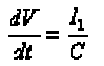 |
| where Il is the leakage current. Thus C should be as large as possible in order to minimize droop The resistance of the FET when turned on (typically tens of ohms) forms a low-pass filter in combination with C and so C should be small if high speed signals are to be followed accurately. Ready-built sample-and-hold circuits are also available as monolithic integrated circuits that simply require the connection of an external hold capacitor. |
 |
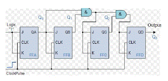
| C. Sunchronous binary counter |
| With the Synchronous Counter, the external clock signal is connected to the clock input of every individual flipflop within the counter so that all of the flip-flops are clocked together simultaneously (in parallel) at the same time giving a fixed time relationship. In other words, changes in the output occur in "synchronization" with the clock signal. This results in all the individual output bits changing state at exactly the same time in response to the common clock signal with no ripple effect and therefore, no propagation delay. In the proposed architecture the synchronous 4 bit counter will increment once for every clock cycle and takes two clock cycles to overflow, so every cycle it will alternate between a transition from 0 to 1 and a transition from 1 to 0. Notice that this creates a new clock with a 50% duty cycle at exactly half the frequency of the input clock. If this output is then used as the clock signal for a similarly arranged D flip-flop one will get another 1 bit counter that counts half as fast. |
 |
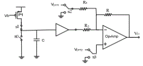
| D. Signal generator |
| A standard analog summing circuit can be used to introduce a shift in the ramp-like signal by adding a small dc voltage to the ramp-like signal. The circuit of Fig. 7 shows one such op-amp based summing circuit. The shift can be added by either closing switch s2 or by closing switch s3. If the gain of the op-amp is sufficiently high, this circuit will provide a constant dc offset but if the op amp gain is not sufficiently high, nonlinearities in the operational amplifier will introduce small nonlinearities in the shift. It is well-known that the offset voltage of an operational amplifier invariably introduces an undesirable shift in the output voltage of most op-amp based circuits.If the offset voltage of an operational amplifier can be controlled by a switch, however, the offset voltage change from when the switch is open to when the switch is closed will provide two signals that are ideally different by a constant shift. The circuit diagram for such a ramp generator is as shown in Fig.7 where switch s3 is used to intentionally introduce mismatch internal to the operational amplifier. The offset voltage in an operational amplifier is comprised of two parts, the systematic part and the random part. The random part, caused by random mismatches and process variations, is not of concern to us. This is because it would be common to both ramp-like signals. Likewise, the systematic part which is common to both ramp-like signals is not of concern either. |
 |
DESCRIPTIONS OF PROPOSED ADC |
| A. Comparator |
| Comparator is desirable to attain the fast conversion. Ramp generator produces the ramp voltage, and it is compared with the comparator input voltage. Finally, comparator generating the hit pulse, if the ramp voltage is better than the input voltage. The difference between the ramp and the input voltage is called as hit pulse. And it passes all the way through the registers and encoders. |
| B. Registers, encoders and multiplexer |
| Clock signals are second - hand for understanding the register values .Two types of registers are READ and WRITE registers. Gray counter and MCG outputs are linked to the encoders. At last step, all data values are composed by means of the multiplexer. Multiplexer perform the operation of first in first out operation(FIFO). |
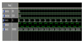
RESULTS AND ANALYSIS OF SPLIT SAR ADC |
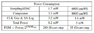
| The power and sampling rate analysis is done by implementing the SARADC in XilinxISE9.2i is shown in Table 1 |
 |
 \ \ |
CONCLUSION |
| Two 1.2 V 10-b SAR ADCs operating at tens of MS/s with additional multiplexer was presented. The linearity behaviors of the DACs switching and structure were analyzed and verified by both simulated and measured results. This switching technique provides superior conversion linearity when compared with the conventional method because of its array’s capacitors correlation during each bit cycling. The proposed coderandomized calibration can eliminate the large DNL and INL errors during switching .Measured results demonstrated that both higher speed and lower power is achieved by using proposed SAR ADC architecture. |
FUTURE WORK |
| Different types of DAC array can be introduced to reduce the linearity erors of SAR ADC. Additional use of capacitive structure may result in improving the conversion efficiency. |
ACKNOWLEDGMENT |
| The authors acknowledge the contributions of the students, faculty of Velalar College of Engineering and Technology for helping in the design of check circuitry,and for tool support.The authors also thank the anonymous reviewers for their thoughtful comments that helped to improve this paper.The authors would like to thank the anonymous reviewers for their constructive critique from which this paper greatly benefited. |
References |
|