Today high-performance microprocessors make use of cache write-through policy for performance improvement and achieving good tolerance to soft errors in on-chip cache. However write through policy incurs large power utilization, while accessing the cache at low level (L2 cache) during write operation. In new method, way_tagged cache was used under write-through policy, it’s consumed more energy. By maintaining the wag tag of L2 cache in the L1 cache during read operation. The proposed technique enables L2 cache to work in direct mapping manner during write hit and reducing tag comparison of cache miss prediction, if cache miss is predicted there is no need to access the L2 cache. So that significant portion of energy will be reduced, without performance degradation. Simulation results are obtained both L1 and L2 cache configuration. The proposed technique achieves 70.7%energy saving in L2 cache on average with only 0.02% area overhead and no performance degradation, when compare with existing methods.
Index Terms |
| Cache, low power, write-through policy,
way tag |
INTRODUCTION |
| Multi-level on-chip cache systems have been
commonly adopted in high-performance microprocessor
[2]-[4]. Cache is the highest or first level of the memory
hierarchy, it store the frequently access data.L2 caches are
unified caches, which has L1 and further data .to keep the
data reliable throughout the memory hierarchy, writethrough
and write-back policies are commonly employed.
Under the write-through Policy, all copies of a cache block
are updated immediately both L1 and L2 after The cache
block is modified at the current cache, even though The block might not be evicted. As a result, the write-through
Policy maintains identical data copies at all levels of the
cache (L1 and L2) hierarchy throughout most of their life
time of execution. |
| While decreasing device sizes radiation produced
soft error, become a serious problem for advanced CMOS
circuits. As CMOS technology is scaled into the nanometer
range, where Soft errors in microelectronic components are
induced either by alpha material or by external irradiation
[1]. These errors, which can occur more often than
permanent errors [5], arise from Single Event multi-bit
Upsets, are getting poorer in on-chip memories [7],[8]. At
the architecture level, an effective solution is to keep data
consistent among different levels of the memory hierarchy
to prevent the system from soft errors [10]–[12]. Benefited
from immediate update, cache write-through policy is
effectively tolerant to soft errors because the data at all
related levels of the cache hierarchy are always kept
consistent. Due to this aspect many high performance
micro-processor designs have adapted write-through policy. |
| Consider a two-level (i.e., L1 and L2) cache
system for example. If the L1 data cache implements the
write-back policy, a write hit in the L1 cache does not need
to access the L2 cache. In contrast, if the L1 cache is writethrough,
then both L1 and L2 caches need to be accessed for
every write operation. Obviously, the write-through policy
incurs more write accesses in the L2 cache then L1 cache,
which in turn increases the energy consumption of the cache
system. So that power consumption is reduced because of
power consumption is a one of the serious issues in
designing cache system [13]-[14]. |
| In this paper, we propose new cache architecture,
referred to as partial way-tagged cache, to improve the
energy efficiency of write-through cache systems with
minimal area overhead and without performance
degradation. Consider a two-level cache hierarchy, where the L1 data cache is write-through and the L2 cache is
inclusive for high performance. It is observed that all the
data present in the L1 cache will have copies in the L2
cache. In addition, the locations of these copies in the L2
cache will not change until they are ejected from the L2
cache. Thus, we can attach a way tag in the L2 cache and
send this tag information to the L1 cache when the data is
loaded to the L1 cache. During the subsequent accesses
when there is a write hit in the L1 cache, we can access the
L2 cache in an equivalent direct-mapping manner because
the way tag of the data copy in the L2 cache is available. As
this operation accounts for the majority of L2 cache
accesses in most applications, the energy consumption of
L2 cache can be reduced significantly. |
| In this paper, the work is extending by making the
following contributions. First, a detailed VLSI architecture
of the proposed way tagged cache is developed, where
various design issues regarding timing, control logic,
operating mechanisms, and area overhead. Second, the idea
of way tagging can be extended to many existing low-power
cache design techniques, so that better tradeoffs of
performance and energy efficiency can be achieved. Finally,
a complete simulations is performed with new results
covering the effectiveness of the proposed technique under
different cache configurations, further improve energy
efficiency. |
BACKGROUND AND RELATED WORKS |
| Many techniques have been developed to reduce
cache power dissipation. In this section, we briefly analysis
some existing work related to the proposed technique. In [6]
partitioned cache data arrays into several sub banks. During
each access only the desired subbank is activated and
corresponding data is activated. Ghose et al. further divided
cache bitlines into small segmentations [9]. When a
memory cell is accessed, only the connected bitline
segmentations are evaluated. These techniques effectively
reduce the energy per access by modifying the structure of
cache systems. At the architecture level, set-associative
caches mostly preferred due to their low miss rates. In
conventional set-associative caches, all tag and data arrays
are accessed simultaneously for performance improvement.
This, however, comes at the cost of energy overhead. Many
techniques have been proposed to reduce the energy
consumption of set-associative cache. The fundamental idea
is to trigger fewer tags and data arrays during an access, so
that cache power dissipation can be reduced. In the phased cache [15] proposed by Hasegawa et al., two phase of cache
access. Cache tag arrays are accessed in the first phase and
the second phase only the data array is access
corresponding to the matched tag. Energy consumption can
be reduced due to only one data array is accessed compare
to the N-data array. Due to the increase in access cycles to
reduce the performance on phased cache this usually
employed in the lower level memory. Another technique
referred to as way concatenation was proposed by Zhang et
al. [16] to reduce the cache energy in embedded systems.
According to the system requirement the cache can be
configured as direct-mapping, four-way, two-way setassociative
with the necessary software support. By
accessing fewer tag and data arrays, better energy efficiency
is attained. This technique is effectively suitable for
embedded system, but not suitable for high-performance
microprocessors. Other techniques include way-predicting
set-associative caches, proposed by Inoue et al. [17]–[19],
that make a prediction on the ways of both tag and data
arrays in which the desired date might be located in cache. |
| If the prediction is correct, the corresponding way
of data array is accessed to complete the operation;
otherwise, the rest ways of the cache are accessed to collect
the desired data. Another similar approach proposed by Min
et al. [20] employs redundant cache to predict the incoming
cache references. The location cache needs to be trigged for
every operation in the L1 cache which wastes energy if the
hit rate of L1 cache is high. Among the above related work,
phased caches and way-predicting caches are commonly
employed in high-performance Microprocessors. Compared
with these techniques, the proposed way-tagged cache
achieves better power efficiency without performance
degradation. Specifically, the basic idea of way-predicting
caches is to store a small number of the most recently used
(MRU) addresses. Since L2 caches are usually unified
caches, so the MRU-based prediction has a poor prediction
rate [21], [22], it reduce the performance. For phased
caches, the energy consumption of accessing tag arrays is
nearly portion of total L2 cache energy. As Shown in
Section III, applying the proposed technique of way tagging
can reduce this energy consumption. Section IV provides
more details comparing the proposed technique with twolevel
cache. |
WAY-TAGGED CACHE |
| In this section, we propose a way-tagged cache that
utilizes the way information in L2 cache to improve energy efficiency. We consider a conventional set-associative
cache system when the L1 data cache loads/writes data
from/into the L2 cache; all ways in the L2 cache are
activated simultaneously for performance consideration at
the cost of energy overhead. Fig. 1 illustrates the
architecture of the conventional two-level cache. Only the
L1 data cache and L2 unified cache are shown. |
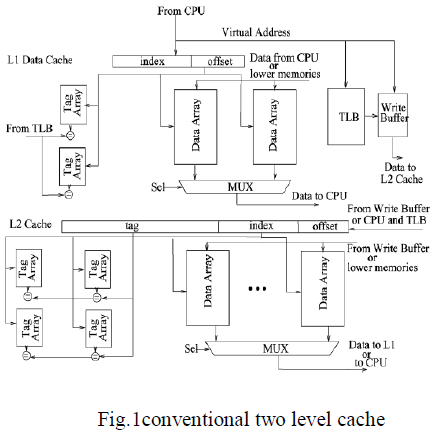 |
| The L2 cache always maintains the most recent copy of the
data under the write through policy. Thus, the L2 cache is a
unified cache, whenever a data is updated in the L1 cache,
the L2 cache is updated with the same data as well. This
will increase the write access in L2 cache and becomes
more energy consumption. |
 |
| The read accesses in the L2 cache are initiated by the read
misses in the L1 cache, which usually occurs much less
frequently. Normally write access consumes more power in
the total power. The location of L1 data copies in the L2
cache will not change until the data are evicted from the L2
cache. The proposed way-tagged cache reduces the number
of ways accessed during L2 cache accesses. The way-tag
arrays stores the way tags of the data in the L2 cache; the L1 data cache loads a data from the L2 cache. These way
tags provide the key information for the consequent write
accesses to the L2 cache. |
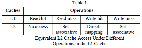
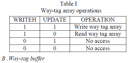
| In general, both write and read accesses in the L1
cache may need to access the L2 cache. These accesses lead
to different operations as summarized in Table I in proposed
method all write operations of the L1 cache need to access
the L2 cache under the write through policy. In the case of a
write hit in the L1 cache, the L2 cache will be activated
only one way because the way tag information of the L2
cache is available in way-tag array. |
| While for a write miss in the L1 cache, the
corresponding data is not stored in the L1 cache. As a result,
its corresponding way tag information is not available in the
way-tag arrays. So, all ways in the L2 cache need to be
activated simultaneously. By this approach all L1 write
operation need to access the correct location in L2 cache in
order to avoid the performance degradation. Note that waytag
arrays are very small in size. For L1 read operation, if
the cache hit means directly access the L1 data no need to
access way-tag array so that significant portion of the
energy is reduced. If cache miss means check the way-tag
array the tag is matched and select correct is activated in L2
cache or else all way are active in L2 cache. Write accesses
account for the majority of L2 cache accesses in most
applications; so that energy overhead is occur in high
performance microprocessor. In addition, write hits are
dominant among all write operations. Therefore, by
activating fewer ways in most of the L2 write accesses, the
proposed way tagged cache is very effective in reducing
memory energy consumption. |
| Fig. 2 shows the system diagram of proposed waytagged
cache. New components are introduced: way-tag
arrays, way-tag buffer, way decoder, and way register, all
shown in the dotted line. The way tags of each cache line in
the L2 cache are maintained in the way-tag arrays, located
with the L1 data cache. Note that write buffers are
commonly employed in write through caches to improve the
performance. With a write buffer, the data to be written into
the L1 cache is also sent to the write buffer. This avoids
write stalls for write operations to be completed in the L2
cache. A small way-tag buffer is introduced to buffer the
way tags read from the way-tag arrays. A way decoder is
working to decode way tags and generate the enable signals
for the L2 cache, which activate only the desired ways in
the L2 cache. Each way in the L2 cache is encoded into a
way tag. A way register stores way tags and provides this
information to the way-tag arrays. |
PROPOSED WAY TAG CACHE |
| Fig.2 shows the diagram of proposed way-tagged
cache architecture. In this paper, introduce several new
components: way-tag arrays, way-tag buffer, way decoder,
and way register, all shown in the dotted line. |
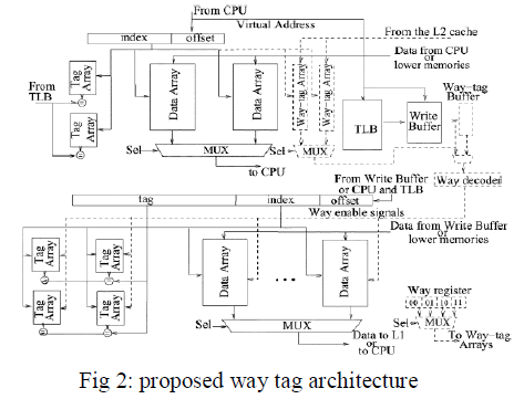 |
| A. Way-Tag Arrays |
| Way tag arrays have way tags of a data is loaded
from the L2 cache to the L1 cache, shown in Fig 3. Note
that the data arrays in the L1 data cache and the way-tag
arrays share the same address from CPU. The WRITEH_W
signal of way-tag arrays is generated from the write/read
signal of the data arrays in the L1 data cache as shown in
Fig. 8. A UPDATE is control signal, obtained from the
cache controller. When a L1 write miss, UPDATE will be
declared and allow WRITEH_W to enable the write
operation to the way-tag arrays (UPDATE=1 and
WRITEH_W, See Table II). UPDATE keeps invalid and
WRITEH_W =1, a read operation to the way-tag arrays.
During the read operations of the L1 cache, the way-tag
arrays do not need to be accessed and thus, reduce energy
overhead. To minimize the overhead of way-tag arrays, the
size of a way-tag array can be expressed as |
 |
Where SL1, Sline,L1 and Nway,L1 are the size of the L1 data
cache, cache line size and number of the ways in the L1 data cache respectively.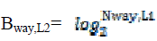 is a binary
code. is a binary
code. |
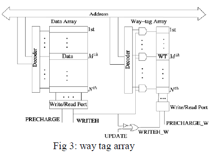 |
| The way-tag arrays are operated in parallel with
the L1 data cache for avoiding the performance degradation.
Due to their small size, the access delay is much smaller
than that of the L1 cache. |
 |
| Way-tag buffer is temporarily stores the Way tags
from the way-tag arrays in the L1 cache. It has the same
number of entries as the write buffer of the L2 cache and
shares the control signals with it. Note that write buffers are
commonly employed, the data to be written into the L1
cache is also sent to the write buffer to improve the
performance. This avoids write stalls when the processor
waits for write operations to be completed in the L2 cache.
When a write miss occurs in L1 cache, all the ways in the
L2 cache need to be activated as the way information is not
available. Otherwise, only the desired way is activated. Way
tag buffer is small in to avoid area overhead. |
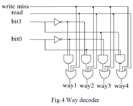
| C. Way decoder |
| The function of the way decoder is employed to
decode way tags and generate the enable signal, which
activate only desired ways in L2 cache. This avoids the
additional wires and the chip area is negligible. A write hit
in the L1 cache, the way decoder works as an n -to- N
decoder that selects one way-enable signal. For a write miss
or a read miss in the L1 cache, the way decoder assert all
way-enable signals, so that all ways in the L2 cache are
activated. A Fig.4 shows that write and read miss signals
decides the way decoder operation. |
 |
| D. way register |
| The way tags for the way-tag arrays is Provided by
Way register. A 4-way L2 cache is consider, that labels
“00”, “01”, “10”, and“11”.This are stored in the way
register. When the L1 cache loads a data from the L2 cache,
the corresponding way tag in the way register is sent to the
way-tag arrays by this manner the corresponding way tags
are stored in way-tag array. The proposed way-tagged
caches way operates under different modes during read and
write operations. Only the way containing the desired data
is activated in the L2 cache for a write hit in the L1 cache,
working the L2 cache equivalently a direct-mapping cache
to reduce energy consumption without performance
overhead under the write-through policy. |
RESULT AND DISCUSSION |
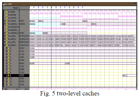
| The way-tag cache has been implemented using
VHDL Language. Fig.3 shows the simulation results for two level caches. Clock, array of tag and data are given as
input, corresponding data are return into the memory or else
read the data from the memory depending upon read and
write operation. |
 |
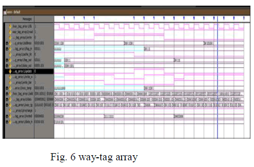
| Fig. 6 shows the simulation results for way tag
array. Clock, array of tag and data are given as input,
corresponding data are return into L1 or else read the data
from theL2 cache depending upon operation cache hit and
cache miss occur in L1 cache. |
 |
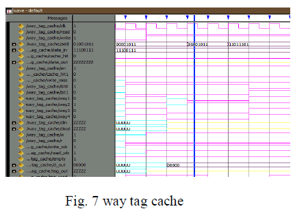
| Fig. 7 shows the simulation results for way tag
cache. Clock, array of tag and data of L1, L2 and way tag
array are given as input, corresponding data are return into
L1 or else read the data from theL2 cache depending upon
operation cache hit and cache miss occur in L1 cache and
way tag array. |
 |
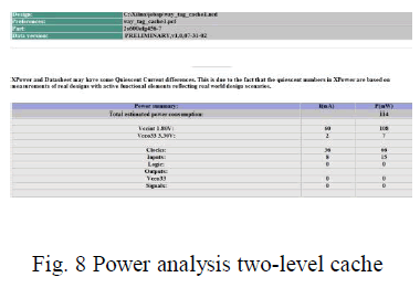
| Fig. 8 shows that power analysis of two-level
cache. This will consumes power 222mW. |
 |
| Fig. 9 shows that power analysis of way tag
caches. This will consumes power 114mW.the operations
way-tagged cache consumes less power compare the twolevel
cache. |
|
| Fig. 9 Power analysis of way tag cache |
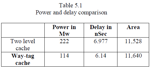 |
| Table 5.1 shows that power and delay comparison
for both two-level cache and way-tag cache. Here, way-tag
cache consumes less power when compare the two-level
cache as well as delay also reduced. Nearly 50% of the
power will be reduced and 10% of delay also reduced. |
CONCLUSION |
| This paper presents a new energy-efficient cache
technique for high-performance microprocessors employing
the write-through policy. The proposed technique has a
way-tag array, it stores to each way in the L2 cache. This
way tag is sent to the way-tag arrays in the L1 cache when
the data is loaded from the L2 cache to the L1 cache.
Utilizing the way tags stored in the way-tag arrays, the L2
cache can be accessed as a direct-mapping cache during the
subsequent write hits, thereby reducing cache energy
consumption. Simulation results demonstrate significantly
reduction in cache energy consumption with minimal area
overhead and no performance degradation. Furthermore, the
idea of way tagging can be applied to many existing lowpower
cache techniques such as the phased access cache to
further reduce cache energy consumption. Future work is
being directed towards extending this technique with partial
tag comparison to reducing the energy consumption of
cache operations. |
References |
- J.F. Ziegler et al., âÃâ¬ÃÅIBM experiments in soft fails in computerelectronics (1978-1994)âÃâ¬ÃÂ, IBM J. Res. Develop., vol. 40, pp. 3 - 18, Jan.1996.
- G. Konstadinidis, K. Normoyle, S. Wong, S. Bhutani, H. Stuimer, T. Johnson, A. Smith, D. Cheung, F. Romano, S. Yu, S. Oh, V.Melamed, S. Narayanan, D. Bunsey, C. Khieu, K. J. Wu, R. Schmitt, A. Dumlao, M. Sutera, J. Chau, andK. J. Lin, âÃâ¬ÃÅImplementation of a third-generation 1.1- GHz 64-bit microprocessor,âÃâ¬Ã IEEE J. Solid-State Circuits, Vol. 37, No. 11, pp. 1461âÃâ¬Ãâ1469, Nov. 2002
- S. Rusu, J. Stinson, S. Tam, J. Leung, H. Muljono, and B. Cherkauer, âÃâ¬ÃÅA 1.5-GHz 130-nm itanium 2 processor with 6-MB on-die L3 cache,âÃâ¬Ã IEEE J. Solid-State Circuits, Vol. 38, No. 11, pp. 1887âÃâ¬Ãâ1895, Nov. 2003.
- D. Wendell, J. Lin, P. Kaushik, S. Seshadri, A. Wang, V. Sundararaman, P. Wang, H. McIntyre, S. Kim, W. Hsu, H. Park, G. Levinsky, J. Lu, M. Chirania, R. Heald, and P. Lazar, âÃâ¬ÃÅA 4 MB on-chip L2 cache for a 90 nm 1.6 GHz 64 bit SPARC microprocessor,âÃâ¬Ã in IEEE Int. Solid-State Circuits Conf. (ISSCC) Dig. Tech. Papers, 2004, pp. 66âÃâ¬Ãâ67.
- C. Su and A. Despain, âÃâ¬ÃÅCache design tradeoffs for power and performance optimization: A case study,âÃâ¬Ã in Proc. Int. Symp. Low Power Electron. Design, 1997, pp. 63âÃâ¬Ãâ68.
- C. Su and A. Despain, âÃâ¬ÃÅCache design tradeoffs for power and performance optimization: A case study,âÃâ¬Ã in Proc. Int. Symp. Low Power Electron. Design, 1997, pp. 63âÃâ¬Ãâ68.
- J. Maiz, S. hareland, K. Zhang, and P.Armstrong, âÃâ¬ÃÅCharacterization of multi-bit soft error events in advanced SRAMs,âÃâ¬Ã in Proc. Int. Electron Devices Meeting, 2003, pp. 21.4.1âÃâ¬Ãâ21.4.4.
- F. X. Ruckerbauer and G. Georgakos, âÃâ¬ÃÅSoft error rates in 65 nm SRAMs: Analysis of new phenomena,âÃâ¬Ã in Proc. IEEE Int. On-Line Test. Symp., 2007, pp. 203âÃâ¬Ãâ204.
- K. Ghose and M. B.Kamble, âÃâ¬ÃÅReducing power in superscalar processor caches using subbanking, multiple line buffers and bit-line segmentation,âÃâ¬Ã in Proc. Int. Symp. Low Power Electron. Design, 1999, pp. 70âÃâ¬Ãâ75.
- G. H.Asadi,V. Sridharan, M. B. Tahoori, andD.Kaeli, âÃâ¬ÃÅBalancing performance and reliability in the memory hierarchy,âÃâ¬Ã in Proc. Int. Symp. Perform. Anal. Syst. Softw., 2005, pp. 269âÃâ¬Ãâ279.
- L. Li, V. Degalahal, N. Vijaykrishnan, M. Kandemir, and M. J. Irwin, âÃâ¬ÃÅSoft error and energy consumption interactions: A data cache perspective,âÃâ¬Ã in Proc. Int. Symp. Low Power Electron. Design, 2004, pp. 132âÃâ¬Ãâ137.
- X. Vera, J. Abella, A. Gonzalez, and R. Ronen, âÃâ¬ÃÅReducing soft error vulnerability of data caches,âÃâ¬Ã presented at the Workshop System Effects Logic Soft Errors, Austin, TX, 2007.
- S. Segars, âÃâ¬ÃÅLow power design techniques for microprocessors,âÃâ¬Ã in Proc. Int. Solid-State Circuits Conf. Tutorial, 2001, pp. 268âÃâ¬Ãâ273.
- A. Malik, B. Moyer, and D. Cermak, âÃâ¬ÃÅA low power unified cache architecture providing power and performance flexibility,âÃâ¬Ã in Proc. Int. Symp. Low Power Electron. Design, 2000, pp. 241âÃâ¬Ãâ243.
- A. Hasegawa, I. Kawasaki, K. Yamada, S. Yoshioka, S. Kawasaki, and P. Biswas, âÃâ¬ÃÅSh3: High code density, low power,âÃâ¬Ã IEEE Micro, Vol. 15, No. 6, pp. 11âÃâ¬Ãâ19, Dec. 1995.
- C. Zhang, F. Vahid, and W. Najjar, âÃâ¬ÃÅA highly-configurable cache architecture for embedded systems,âÃâ¬Ã in Proc. Int. Symp. Comput. Arch., 2003, pp. 136âÃâ¬Ãâ146[20] K. Inoue, T. Ishihara, and K. Murakami, âÃâ¬ÃÅWay predicting set-associative cache for high performance and low energy consumption,âÃâ¬Ã in Proc. Int. Symp. Low Power Electron. Design, 1999, pp. 273âÃâ¬Ãâ275.
- A.Ma, M. Zhang, and K.Asanovi, âÃâ¬ÃÅWay memoization to reduce fetch energy in instruction caches,âÃâ¬Ã in Proc. ISCA Workshop Complexity Effective Design, 2001, pp. 1âÃâ¬Ãâ9.
- T. Ishihara and F. Fallah, âÃâ¬ÃÅA way memoization technique for reducing power consumption of caches in application specific integrated processors,âÃâ¬Ã in Proc. Design Autom. Test Euro. Conf., 2005, pp. 358âÃâ¬Ãâ363.
- R. Min, W. Jone, and Y. Hu, âÃâ¬ÃÅLocation cache: A low-power L2 cache system,âÃâ¬Ã in Proc. Int. Symp. Low Power Electron. Design, 2004, pp. 120âÃâ¬Ãâ 125.
- B. Calder, D. Grunwald, and J Emer, âÃâ¬ÃÅPredictive sequential associative cache,âÃâ¬Ã in Proc. 2nd IEEE Symp. High-Perform. Comput. Arch., 1996, pp. 244âÃâ¬Ãâ254.
- T. N. Vijaykumar, âÃâ¬ÃÅReactive-associative caches,âÃâ¬Ã in Proc. Int. Conf. Parallel Arch. Compiler Tech., 2011, p. 4961.
|