International Journal of Innovative Research in Science, Engineering and Technology
ISSN ONLINE(2319-8753)PRINT(2347-6710)
ISSN ONLINE(2319-8753)PRINT(2347-6710)
S.R. Reddy1, Rahul Prasad2, Abhishek Sharan2 and B. Prasad3
|
| Related article at Pubmed, Scholar Google |
Visit for more related articles at International Journal of Innovative Research in Science, Engineering and Technology
In the fabrication of crystalline (mono and multi) silicon solar cells, p-type silicon wafers are diffused with phosphorous to form large area (240 Cm2) p-n junction, which is responsible for separation of photo generated carriers. During emitter diffusion process, phosphorous diffusion also takes place over the edges and rear side of the wafer. This creates shunt paths between the front (n-type) and back (p-type) surface. These shunt paths cause reduction in solar cell efficiency. In the study presented here, Q-switched nanosecond 532 nm wavelength laser is used for isolating the shunts at the edges by scribing on either front or back side of cells. The effect of laser scribing parameters on groove characteristics is studied and optimized so as to get maximum efficiency of solar cells. From our results, we find that laser edge isolation process shows an enhancement of average output power of solar cells by 3.45% compared to the plasma edge isolation process. The laser edge isolation technique developed is suitable for inline production for industrial applications and is environment friendly as no hazardous fluorine based chemicals are used.
Keywords |
| Edge isolation, Laser, Solar Cells |
INTRODUCTION |
| In solar cell manufacturing, p-type boron doped wafers are diffused with phosphorous to form a large area p-n junction, which is required to separate the photo generated carriers. During the diffusion process, phosphorous diffusion takes place on both sides and as well as on the edges of the cell. This parasitic emitter diffusion that wraps around the wafer edges creates shunt paths. These shunt paths are eliminated by edge isolation process. There are different methods, such as plasma etching, dispensing of etching paste, wet chemical etching, mechanical scribing, laser scribing etc., to perform edge isolation on silicon solar cells [1]. Conventionally in solar cell manufacturing industries, edge isolation is done by plasma etching. In this process, diffused Si wafers are coin-stacked and tightly held between two plates to expose only the edges to fluorine based plasma in a reactor and thereby etching off the shunt paths. This step is not an in-line process and requires use of hazardous chemicals. In-line wet chemical etching is another method used in the industry that uses hazardous chemicals and too many cleaning processes.Therefore, there is a demand for alternate options that can be performed in-line and are easy to implement cost effectively without the use of hazardous chemicals. A few groups are working to develop edge isolation process by laser which has in-line capability and is also environmental friendly as no hazardous chemicals are used [1, 2]. In laser edge isolation, a continuous groove is scribed through the n-type layer along the periphery of cell to achieve electrical isolation.This groove should be narrow and as close as possible to the edge in order to maximize the cell’s active area.Few authors [3-4] reported laser edge isolation process using 1064 nm IR laser, but it is also reported that on ablation of silicon, some micro cracks are observed that emanate from the scribed groove and moreover, the scribed groove width is also wider compared to the groove made by 532 nm wavelength laser [2]. Hence, to overcome these issues manufacturers are turning to 532 nm and 355 nm lasers to improve the performance of solar cells. In this study, we employed Q switched nanosecond 532 nm laser to perform edge isolation as this laser can scribe narrow grooves and cause less damage to Si wafer. |
EXPERIMENTAL |
| A. Solar cell fabrication |
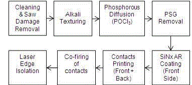
| Conventional process steps shown in Fig.1 are followed for the fabrication of mono-crystalline Si solar cells. Texturing of p-type silicon wafers (156 mm × 156 mm) is carried out in an alkali bath. The textured wafers are diffused with phosphorus in an open-tube furnace using a conventional POCl3 diffusion source followed by phosphosilicate glass (PSG) removal by chemical etching. The sheet resistance of resulting emitter is in the range of 30-40 Ω/sq. An anti reflection coating of 80-nm thick SiNx layer is deposited by plasma-enhanced chemical vapor deposition (PECVD) method. The refractive index of the SiNx film is maintained at around 2.0. The front and back metallization is carried out using a screen printing technique with standard silver and aluminum pastes. This is followed by baking and cofiring of the contacts in a conveyer belt furnace. Finally, the laser edge isolation is performed by scribing a groove on either front or back side of the cell. The laser grooves are characterized by scanning electron and optical micrographs. The present laser edge isolation scheme is shown in Fig. 2. The cells are characterized by using I-V characteristics measured by I-V measurement setup. The I-V measurement set up has the provision to measure I-V characteristics of a solar cell in dark and under illumination. The solar cell to be tested is firmly held on a gold-plated, temperature controlled vacuum chuck and the measurement of current and voltage are made with 4-wire arrangement (2 wires for current and 2 separate wires for voltage). For all measurements under illumination, first the light intensity is checked and adjusted to 100 mW/cm2. Also, the temperature of the chuck is set at the desired temperature with tolerance of ±1 °C and monitored continuously using a PT100 probe inserted horizontally inside the gold plated chuck. Calibration of the intensity is performed with the help of the reference cell calibrated at NREL, USA (Make: PV Measurements Inc. USA, Model No.: PVM 230, 4 cm2 area, Isc: 107 mA @ 25±0.2 °C, mounted on an Al block with BK7 glass protective window, with 4 wire contacts). The reference cell is certified for use to quantify or set the irradiance level of a light source used for testing solar cells and modules. When the short circuit current out put of the reference cell is equal to its calibrated value of short circuit current, it indicates that the irradiance reaching the reference cell is equivalent to the irradiance (usually one sun) that was present during its calibration. The I-V measurement system comprises a controller module which interfaces with a power supply / electronic load on one hand and a PC on the other from where the parameters of measurements are set. The system operates with the help of embedded data acquisition and analysis software to sweep the forward light I-V characteristics and forward dark log J-V curves. |
 |
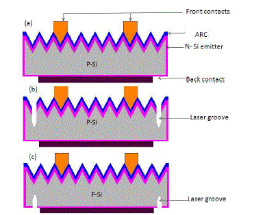 |
| B. Laser Edge Isolation |
| A Q-switched nanosecond laser with 532 nm wavelength is used to scribe a groove at a distance of 0.3 mm from the edges of the wafer on either front or back side of the solar cell. The cell is mounted on a vacuum chuck and the laser beam is focused onto the wafer through the f-θ lens. Using the galvo scanner, the laser beam is moved to scribe a groove along the periphery of the solar cell. The repetition frequency of laser was kept constant at 50 kHz as it was found to be most stable at this frequency. There are a number of laser parameters that needs to be optimized for this process, namely, laser power, laser speed and number of repetitions. |
RESULT AND DISCUSSIONS |
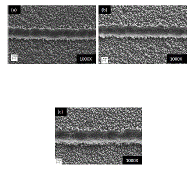
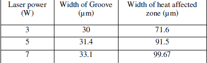
| In order to optimize laser parameters suitable for edge isolation, several experiments are carried out by scribing grooves under various laser power settings. To optimize the scan speed it is to be ensured that there is sufficient overlap between the consequitive laser pulses. The scan speed is kept constant at 100 mm/s for scribing the groove since we attain a continuous groove. The grooves are characterized by scanning electron and optical micrographs. The scanning electron micrographs taken for grooves scribed with average laser power of 3.5 W, 5 W and 7 W are shown in Fig.3. It can be seen from Fig.3 that the grooves are continuous and the depth of the groove increases relatively on increasing the laser power. |
 |
 |
 |
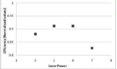
| In order to see the effect of laser power on solar cell performance, laser edge isolation is carried out on front side with one repetition cycle for various laser powers. For each laser power setting, five cells were scribed and average values of cell efficiency relative to plasma edge isolated cells are shown in Fig.4. The solar cell performance is characterized by I-V measurement and their efficiency is compared. From Fig.4, it is clear that the cells scribed with 4W power show low efficiency compared to the cells scribed with moderate laser power (5-6 W) because of incomplete isolation. It can also be seen from the Fig.4, that the cells scribed with higher laser powers (>6W) show decrease in cell efficiency. This could be due to damage caused by overheating of Si. However, in this set of experiments, all the laser edge isolated cells show low efficiency and fill factor values compared to plasma edge isolated cells. This indicates that the shunt paths are not completely isolated. The possible reason for this is that the depth of the groove is not sufficient to isolate the emitter completely leading to incomplete edge isolation. |
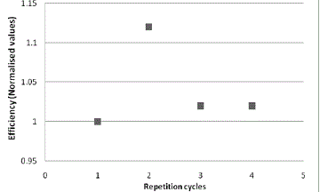 |
| Repetition cycle is another laser parameter which affects the depth of groove without inducing overheating effects. Therefore, another set of experiments are carried out by increasing the number of repetition cycles at a constant laser power of 5W. The average values of cell efficiency for the cell scribed with laser power 5 W under different repetition cycles are shown in Fig.5. |
 |
| It can be seen from Fig.5 that the cells isolated with 2 repetition cycles show improvement in cell efficiency and fill factor due to complete isolation of shunt paths. However, the cells scribed beyond two repetition cycles shows low efficiency, this could be due to damage induced by the laser along the scribe line. Therefore, two repetition cycles are good enough to isolate the emitter layer completely. |
| Based on the above experiments, it is seen that the cells scribed with 2 repetition cycles at 5 W power show better efficiency and fill factor values. Therefore, two batches of cells (each batch having 100 nos.) are edge isolated under above conditions. One batch is scribed on front side and another batch on rear side and the performance of these cells are compared with 100 nos. of plasma edge isolated cells. The average cell performance parameters relative to plasma edge isolated cells are given in Table-2. |
| Table-2.Comparison of solar cell parameters of laser and plasma edge isolation |
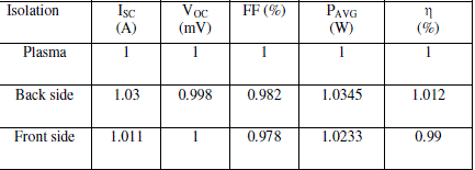 |
| From Table-2, it can be seen that rear side edge isolation yields better efficiency compared to front edge isolation because there is gain in front active area which improves the short circuit current leading to improvement in cell efficiency. It can also be seen that average output power of a solar cell is increased by 3.45% on scribing with laser as compared to plasma edge isolation. |
CONCLUSION |
| Edge isolation is an important step in the solar cell process. In industries, edge isolation is carried out by either plasma etching or chemical edge isolation. Laser edge isolation is fast and compatible with the inline process for industrial solar-cell fabrication. In the reported work, front and rear side laser edge isolation is successfully carried out using a 532 nm DPSS laser. Edge isolation at a distance of 0.3 mm from the edge of the wafer with optimized laser parameters yield the best result. It is observed that the laser edge isolation process show enhancement of average output power of cells by 3.45 % over plasma edge isolation process. In addition, the laser edge isolation technique is environmental friendly as no hazardous fluorine based chemicals are used. Thus, laser edge isolation done at a scribing speed of 100 mm/s is compatible with inline industrial cell fabrication after incorporating automatic loading and unloading mechanisms. |
ACKNOWLEDGEMENTS |
| The authors are thankful to the BHEL management for their constant encouragement during the project implementation and permission to publish this work. |
References |
|