International Journal of Innovative Research in Science, Engineering and Technology
ISSN ONLINE(2319-8753)PRINT(2347-6710)
ISSN ONLINE(2319-8753)PRINT(2347-6710)
Wilayat Khan1, Sikander Azam1, Saleem Ayaz Khan1, A. H. Reshak1,2
|
| Corresponding author: Wilayat Khan |
| Related article at Pubmed, Scholar Google |
Visit for more related articles at International Journal of Innovative Research in Science, Engineering and Technology
The electronic structure, electronic charge density and optical properties of the organic –inorganic hybrid semiconductor C2H6NTeZn are premeditated by employing the full-potential density-functional technique. The band structure of our optimize crystal indicate semiconductor nature. For understanding the nature of chemical bonding in the investigated material, we calculate the electronic charge density in (110) and (010) crystallographic planes. From the analysis density of states, we emphasize that in the partial density of states, the valence band maximum is contributed strongly from the Zn-d state and a minor contribution from the hybridization of N-s and C-s states. The conduction band minimum is mainly formed from the Zn-s orbital while on the other hand small contribution from Te-p and Te-s states. Further more, we also have calculated the optical properties, to get a physical basis for latent application in optoelectronic devices.
Keywords |
| Band structure; Density of states; electronic charge density; Optical properties: DFT |
INTRODUCTION |
| Crystalline mixtures constructed up of periodically ordered nanostructured inorganic semiconductor motifs and organic molecules are an innovative kind of hybrid semi conducting components that are of large basic significance and technological relevance [1-9]. The mainly interesting characteristic of these components is that many complimentary properties of each individual constituent are conveyed into the hybrid structure by embedding two noticeably different constituents into a single crystal lattice. Integration and blending of outstanding transport properties and structural/thermal firmness from the inorganic constituent and excellent flexibility and possibility from the organic constituent can be anticipated. Moreover, the combining of the inorganic and organic modules in these crystalline hybrid molecules takes location at the atomic level and through chemical bonds, and therefore is free of the interface issues that are unavoidably present in accepted hybrid composite components. In addition, the configuration of such hybrid crystals nearly always leads to exclusive and remarkable new characteristics that are not possible for the one-by-one constituents. Some prominent demonstrations include organic– inorganic perovskite-like structures and associated materials [1-4] hybrid metal oxides [5, 6] and semiconductors created of zinc blende and wurtzite frameworks [7-9]. The II/VI based hybrid semiconductor crystal structures (II: Group 12 components and Mn; VI: Group 16 components) are composed of one-dimensional (1D) chains or two-dimensional (2D) slabs of II/VI semiconductor fragments that are interconnected or divided by organic amine substances to form periodic crystal lattices. They are of the common equation [MQ(L)x] (M=Mn, Zn, Cd; Q=S, Se, Te; L=organic amine or diamine; and x=0.5, 1). The most captivating explanation encompass exceedingly powerful band-edge absorption (e.g. 10–20 times higher than bulk II/VI and GaAs) and remarkably large band-gap tunability (0.1–2.0 eV) as a consequence of very powerful structure-induced quantum confinement [10, 12] even though, according to theoretical computation [10], the organic spacers grant rise to a very restricted effect on the band-gap-related electrical devices and optical properties, they play a vital function in the structural, mechanical, and thermal behaviors of these hybrid components. In 2009 Xiaoying Huang et. al. [11] reported five crystal structures of 3D-[ZnTe(L)0.5] prepared of ZnTe single-atomic slabs and long chain diamines, in addition to their functional stage transitions, mechanical properties, accurate heat capability, thermal diffusivity, and thermal conductivity. Our analysis displays that crystalline hybrid semiconductors of this kind are much lighter and considerably more bendable than their inorganic corresponding items. The amalgamation of organic substances into the semiconductor crystal lattices also leads to drastically decreased thermal conductivity that is most attractive for high concert thermoelectric materials with functional integrity [12-16]. In this article, we analyze the electronic structure, electronic charge density and optical properties of C2H6NTeZn compound within the modified Becke and Johnson (mBJ) [17] exchange correlation energy within the framework of full-potential linearized augmented plane wave (FP-LAWP) technique as employed in the WIEN2K package [18]. |
II. CRYSTAL STRUCTURE AND COMPUTATIONAL DETAIL |
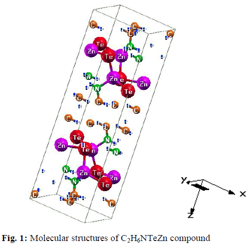
| For our calculations we use the lattice parameters of the organic –inorganic hybrid semiconductor a-ZnTe(bda)0.5, given in the crystallographic data (CCDC-736292) [19]. Our investigated compound has monoclinic symmetry with space group P21/c , having eight formulas/unit cell. The molecular structure of the investigated compound, is shown in Fig. 1. The full-potential linearized augmented plane wave (FP-LAPW) technique is used to calculate the electronic structure and linear optical properties of C2H6NTeZn compound, which is based on density functional theory (DFT) as employed in the WIEN2K package [20]. We carried out the DFT calculations for optimizing the structure of our investigated compound by minimizing the forces acting on each atom of C2H6NTeZn compound to get stable geometry. The structure of the crystal is considered to be stable when the convergence of energy criterion 1mRy/a.u. The self consistency is achieved at 10-4Ry. For our calculations, we choose the RMT values in such a way that no charge leakage is observed from the core and also the convergence of the total energy was ensured. The Muffin Tin (MT) sphere is expanded up to lmax=10, inside which the potential and charge density is indicated. We set the value RMTKMAX=7, for the expansion of the basis function. The electronic exchange-correlation energy is solved by using local density approximation (LDA) [21], generalized gradient approximation (GGA) [22] and Engle Vosko generalized gradient approximation (EV-GGA) [23]. In order to avoid the underestimation of LDA and GGA, we have used the modified Becke-Johnson approximation (mBJ) to get better band gap value. The below equation give mBJ potential and its explanation is found in the Refs [24, 17, 25]. |
 |
 |
III. RESULTS AND DISCUSSION |
Electronic structure |
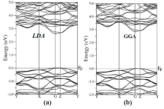
| To examine the electronic and optical properties of a compound, it is very useful to investigate the band structure. The band structure has been calculated for the investigated compound using LDA, GGA, EVGGA and mBJ (see Fig. 2). |
 |
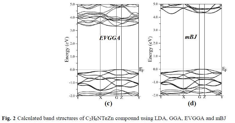 |
| Figure 2 (a, b, c and d), shows the band structure of the investigated compound along the selected high-symmetry lines within the first Brillouin zone of the monoclinic crystal. The symbols is assign to high symmetry points of irreducible Brillioun zone (IBZ). Following Fig. 2, it is clear that our investigated compound is a direct band gap semiconductor. From these results, we conclude that mBJ give better band gap value [27-31] as compared to other approximation i.e. LDA, GGA and EVGGA. Due to this reason, mBJ is taken as a best tool for calculating the band gap. The calculated energy band gaps for the four approximations (LDA, GGA, EVGGA and mBJ), are displayed in the Table 1. |
 ' ' |
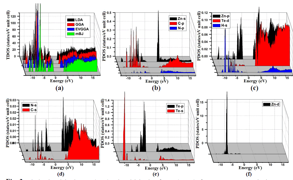
| From the total density of states (TDOS) and partial density of states (PDOS), we can visualize the atomic states hybridization and contributions to the band in the band structure of C2H6NTeZn compound. Fig. 3(a, b, c, d, e and f), report the calculated TDOS by using LDA, GGA, EVGGA and mBJ approximations. Since we state that the mBJ give better band splitting thus for the calculation of PDOS we have demonstrated the results obtained by mBJ (Fig. 3). We emphasized that in the PDOS, the valence band maximum (VBM) is contributed strongly by the Zn-d states with a minor contribution of N-s and C-s states and possess a strong hybridization between N-s and C-s states. Fig. 3, shows that the energy range from -5.0 eV to 0.0 eV is mainly due to the contribution of Te-p, Zn-s and N-p states along with the small contribution of the remaining states. The lowest part of the valence band from -10.0 eV to -5.0 eV is due to the Te-s and Zn-d states provide the greater contribution as compared to other states i.e N-s, C-s, Zn-s, Zn-p, H-s and Te-p, Te-d, which show negligible contribution (Fig. 3). The conduction band minimum is mainly fromed from the Zn-s orbital with the small contribution of Te-p and Te-s states. |
 |
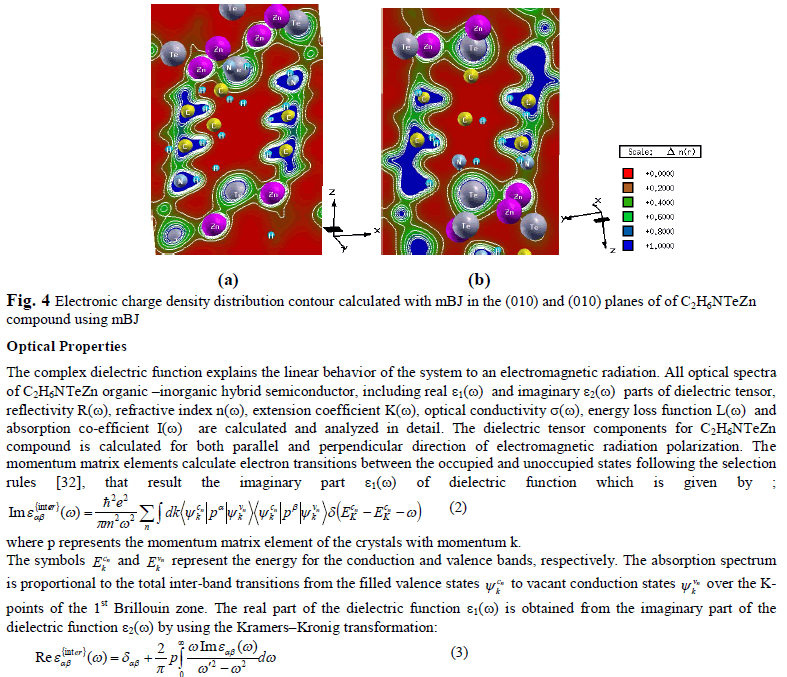
| Electronic charge density In order to understand the chemical bonding nature of the organic –inorganic hybrid semiconductor C2H6NTeZn, we calculate the electronic charge density using mBJ approximation in (110) and (010) crystallographic planes (Fig. 4(a, b). It is clear from the Fig. 4, that Te atom shows ionic nature of chemical bonding, which surround by spherical lines. The values of electro negativity of Carbon, Hydrogen, Nitrogen, Tellurium, and Zinc are 2.55, 2.20, 3.04, 2.1 and 1.65, respectively. The electronegativity difference between two atoms is used to find the bonding nature. The electronegativity difference between Te and Zn is 0.94, which indicate polar covalent bond. On the other hand, the difference in the electronegativity of C and H atoms is 0.30 show strong sharing of electrons and the same bond is also appeared between N and H atoms. It is also clear from the Fig. 4, that there is polar covalent bond between Zn and C atoms. According to thermoscale, the blue color represents greater concentration of charge (+1.0000), that’s why the carbon atom displays maximum charge concentration as compared to other atoms. The crystallographic planes (110) and (010) show considerable anisotropy (see Fig. 4). |
 |
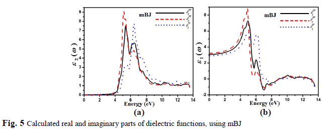
| The inter-band transition is taken into account during the calculation of the real and imaginary part of the dielectric function of C2H6NTeZn compound for parallel and perpendicular direction of electric field, is shown in Fig. 5, using mBJ. Our investigated crystal C2H6NTeZn possess monoclinic symmetry, therefore it contains three nonzero principal dielectric tensor components of second order, as follow xx(), yy() and zz(). Fig. 5a, shows the plots of ( ) 2 xx , ( ) 2 yy and ( ) 2 zz , which is obtained by using mBJ approximation. The imaginary part () of dielectric function indicates several peaks in the energy range from 4.6 to 7.0 eV and the main peaks appeared at 5.37 eV for ( ) 2 xx , 5.14 eV for ( ) 2 yy and 6.4 for ( ) 2 zz originated due to the transitions from Te-p states to Zn-s states. A considerable anisotropic behavior is found among the three spectral components of dielectric tensor (Fig. 5a). |
| The real part of the dielectric tensor components ( ) 1 xx , ( ) 1 yy , and ( ) 1 zz , as shown in the Fig. 5b. The calculated static values of the three components (0) 1 xx , (0) 1 xx and (0) 1 xx are 3.07, 3.24 and 2.91, respectively. Our investigated compound possess a band gap of about 4.26 eV, resulting smaller value of (),which is explained on the basis of Penn model [33]. The Penn model is given by the following relation; 2 (0) 1 g E (4) It is clear from equation (3) that () is inversely proportional to Eg. The compound which has smaller value of band gape exhibit larger value of (). |
 |
IV. CONCLUSION |
| We studied the electronic structure, electronic charge density and linear optical properties of the organic–inorganic hybrid semiconductor C2H6NTeZn, using the first principles calculation. Our calculated results for the band structure indicate direct band gap of about 4.25 eV, using mBJ, which provide better band splitting than the other three approximations. The Te-p, Zn-s and N-p states possess main contribution to the upper part of the valence band, while the lower part of the conduction band is highly contributed by Zn-s orbital with the small support of Te-p and Te-s states. Our calculated electronic charge density repots strong sharing of electrons between C/N with H atoms. We examine that our calculated optical properties show anisotropic nature at the middle of the spectral region. The calculated results of the optical properties show that the C2H6NTeZn is suitable for optoelectronic devices. |
Acknowledgements |
| This result was developed within the CENTEM project, reg. no. CZ.1.05/2.1.00/03.0088, co-funded by the ERDF as part of the Ministry of Education, Youth and Sports OP RDI program. School of Material Engineering, |
References |
|