International Journal of Innovative Research in Science, Engineering and Technology
ISSN ONLINE(2319-8753)PRINT(2347-6710)
ISSN ONLINE(2319-8753)PRINT(2347-6710)
Dheivanai. R1, Thamilarasi. E2
|
| Related article at Pubmed, Scholar Google |
Visit for more related articles at International Journal of Innovative Research in Science, Engineering and Technology
in this paper, a novel technique used to balancing the capacitor voltage of neutral point clamped inverter without transformer and also reduces the total harmonic distortion at the output by using multi carrier pulse width modulation technique. This paper presents orientation of higher order harmonics of fifteen level neutral point clamped inverter. The total harmonic distortion will be carried out using fast Fourier transformation. The effectiveness of the proposed method is verified by simulations.
Keywords |
| FACTS, IGBT, multilevel, multi carrier PWM, NPC inverter, total harmonic distortion. |
INTRODUCTION |
| The necessity of increasing power quality in the past years leads to the development of inverter due to its efficiency and control methods. An inverter is a device which converts the direct current (DC) into an alternating current (AC) without changing the magnitude. The converted current may contain the required voltage and frequency, switching devices and control circuits. In order to improve the quality of an inverter by performs the power conversion of small voltage steps resulted in lower harmonics. The output voltage of an AC side contains several numbers of discrete levels of equal magnitude. |
| The harmonic content of a multilevel inverter is reduced compared to inverter voltage waveform. This method is known as multilevel inverter. Multilevel inverters are significantly different from the ordinary inverter where only two levels are generated. The semiconductor devices are not connected in series for one single high-voltage switch. In which each group of devices contribute to a step in the output voltage waveform. The steps are increased to obtain an almost sinusoidal waveform. The number of switches involved is increased for every level increment. Multi-level power inverters employ power semiconductor switches in the inverter to select the DC voltage source to produce a staircase voltage waveform at the output of inverter. The output of a multilevel inverter is in the form of staircase waveform, so that the harmonics get reduced thereby the voltage gain get increased and the power quality increases. |
| The general purpose of the multilevel inverter is to synthesize a nearly sinusoidal voltage from several levels of dc voltages, typically obtained from capacitor voltage sources. As the number of level increases, the synthesized output waveform has more steps, which produce a staircase wave that approaches a desired waveform. Also as more steps added to the waveform, the harmonic distortion of the output waveform decreases, approaching zero as the level increases. As the number of level increases, the voltage that can be summing multiple voltage levels also increases. |
| Several multilevel inverter topologies are proposed over the past few years, the most popular multilevel inverters which are mostly used are Diode-clamped, Flying capacitor and the H-bridge multilevel inverter. Neutral Point Clamped Inverter is more preferred than other topology. In this paper is concentrated for the improvement of output voltage waveform, reduction of harmonics and for reactive power compensation by using multi carrier pulse width modulation (PWM) technique. It used to balance the dc split voltage and improve the efficiency of the system and reduce the voltage fluctuation. To take benefit of the advantages of the multilevel inverter, Low Electromagnetic interference, Low Total harmonic distortion, reduce conversion losses, it is used to boost the voltage based on the requirement, Reduce Switching losses. |
| In the proposed system Multi Carrier Pulse Width Modulation is used to control the dc split capacitor and reduce the harmonics. The simulation of the proposed control method will be carried out using Mat lab simulation tool wherein the detailed analysis and design aspects can be emphasized. |
NEUTRAL POINT CLAMPED INVERTER |
| In response to the growing demand for high power inverter units, multilevel inverters have been attracting growing attention from academia as well as industry in the recent decade. The multilevel inverter refers to using a converter in the inverting mode. Power can flow from DC side to AC side. |
| Multilevel inverters are extensively used in medium voltage levels with high-power applications. The field applications include use in laminators, pumps, conveyors, compressors, fans, blowers, and mills. Subsequently, several multilevel converter topologies have been developed. Multilevel inverter is a power electronic device built to synthesize a desired ac voltage from several levels of dc voltages. Such inverters have been received increasing attention in the past few years for high power application. A small total harmonic distortion is the most important feature of these inverters. In the adjustable speed drive application, the multilevel inverters can be used for a utility compatible adjustable speed drive (ASD) with the input from the utility constant frequency AC source and the output to the variable frequency AC load. The major differences when using the same structure for ASDs and for back-to-back interties are the control design and the size of the capacitors. Because the ASD need to operate at different frequencies, the DC link capacitor needs to be large enough to avoid a large voltage swing under transient state. |
| Among the best known topologies are the H-bridge cascade inverter, the capacitor clamping inverter (imbricate cells), and the neutral point clamped inverter. As reported in the literature, the NPC inverter has been used in several practical instances for broadcasting amplifier, plasma, industrial drive as well as FACTS applications etc. |
| For FACTS application the power pulsation at twice output frequency occurring with the dc link of each Hbridge cell necessitates over-sizing of the dc link capacitors. The capacitor clamping inverter, though the three-level scheme of which was published in the early 1980’s had been rarely discussed until the introduction of the “imbricate cells”. The individual clamping capacitor needs only to smooth the switching frequency ripple voltage and the required capacity for each clamping capacitor is therefore small. However, as the number of level increases, such problems as thermal designing, lowinductance designing, as well as insulation designing of the system will become critical. |
 |
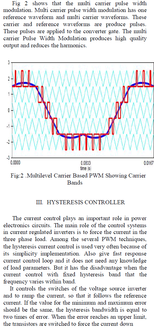
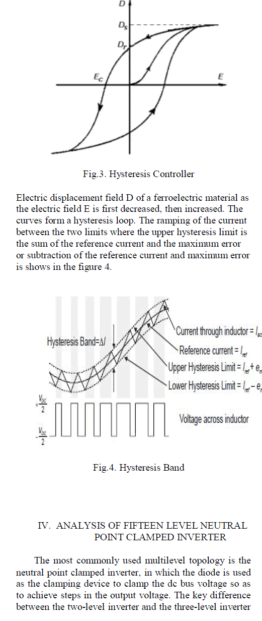
| The neutral point clamped inverters provide high quality output, low switching frequency and high voltage capability. But these features are obtained when the dc split voltage is balanced. To balance the dc split voltage used pulse width modulation. In this project multi carrier pulse width modulation is used and hysteresis controller is used. This controller is used to avoid unwanted rapid switching. The hysteresis controller is very popular because of its inexpensive, simple and easy to use. And also the total harmonic distortion is reduced by using of multi carrier pulse width modulation technique. |
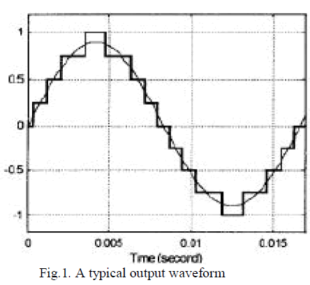
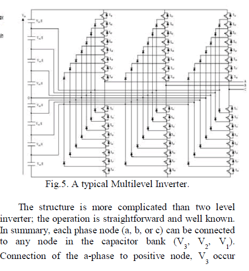
| PWM techniques minimize the magnitude of the harmonics but not removed completely. The multilevel inverter is used to remove the particular harmonics completely. Fig 1 shows the multi level inverter waveform. In the multi level inverter the output level equal to the source which I applied to the inverter. In this diagram sinusoidal waveform and multilevel approximation is indicated. |
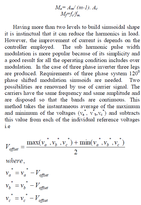
MULTI CARRIER PULSE WIDTH MODULATION |
| Multi Carrier pulse width modulation is the extension of two level carrier based modulation. The multi carrier pulse width modulation technique consists of one reference signal and several triangular carrier signals. The basic principle of multi carrier pulse width modulation (MC-PWM) is comparison reference waveform with carrier waveform. To generate m level it required m-1 carrier. Both carrier and reference signals have same frequency and amplitude. A frequency of sine reference waveform is fr and peak to peak value of reference waveform is Ar. Each carrier is compared with modulating signal at every instant. If the triangular carrier is greater than reference signal the result is 1 otherwise 0. Sum of the different comparison which represents voltage level is output modulator. The scheme is characterized by amplitude modulation index ma and frequency modulation index mf. |
| For a sine waveform (reference) cantered in the carrier bands, the duration of time that the waveform exists. For an m-level inverter, m-1 carriers with the same frequency fc and the same amplitude Ac are disposed such that the bands they occupy are contiguous. The reference waveform has peak-to-peak amplitude Am, a frequency fm, and its zero centred in the idle of the carrier set. The reference is continuously compared with each of the carrier signals. If the reference is greater than a carrier signal, then the active devices corresponding to that carrier is switched on; and if the reference is less than a carrier signal, then the active devices corresponding to that carrier is switched off. In multilevel inverters, the amplitude modulation index, ma, and the frequency ratio, mf, are defined as |
 |
 |
 |
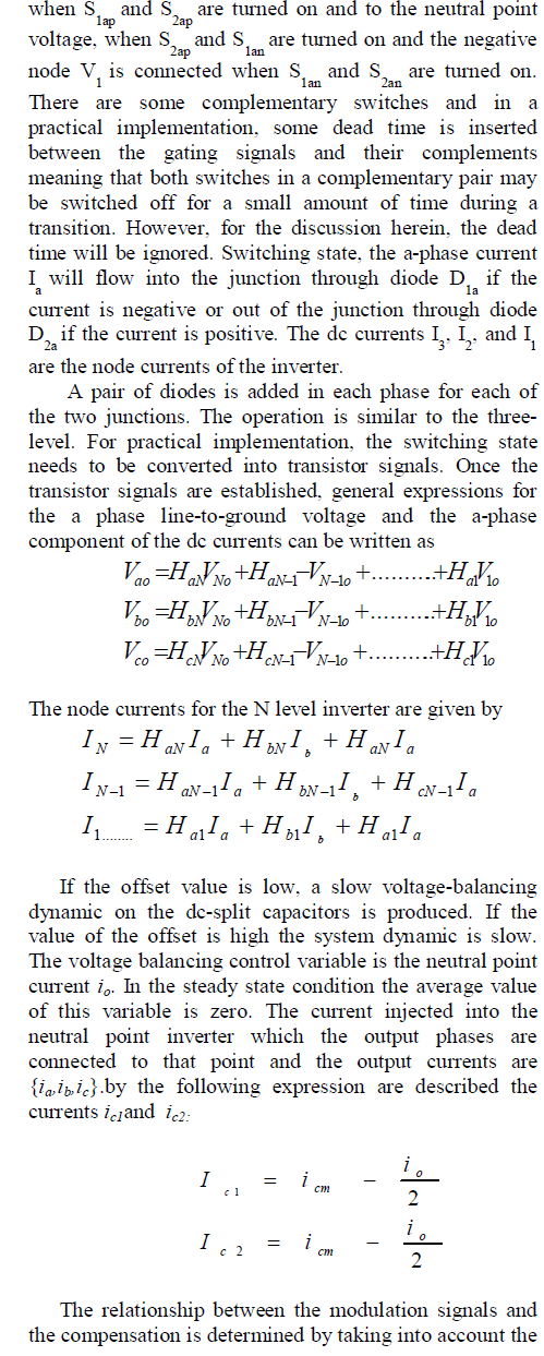
| are the diodes D1a and D2a. These two devices clamp the switch voltage to half the level of the dc-bus voltage. In general the voltage across each capacitor for an N level diode clamped inverter at steady state is 1/− n dc V. Although each active switching device is only required to block V, the clamping devices have different ratings. |
| The neutral point clamped inverter provides multiple voltage levels through connection of the phases to a series of capacitors. According to the original invention, the concept can be extended to any number of levels by increasing the number of capacitors. Early descriptions of this topology were limited to three-levels where two capacitors are connected across the dc bus resulting in one additional level. The additional level was the neutral point of the dc bus, so the terminology neutral point clamped (NPC) inverter was introduced. Due to capacitor voltage balancing issues, the neutral point clamped inverter implementation has been limited to the three levels. Because of industrial developments over the past several years, neutral point clamped inverter is now used extensively in industry applications. |
| In general for an N level diode clamped inverter, for each leg 2 (N-1) switching devices, (N-1) * (N-2) clamping diodes and (N-1) dc link capacitors are required. When N is sufficiently high, the number of diodes and the number of switching devices increase and make the system impracticable to implement. If the inverter runs under pulse width modulation (PWM), the diode reverse recovery of these clamping diodes becomes the major design challenge. |
 |
 |
 |
 |
 |
CONCLUSION |
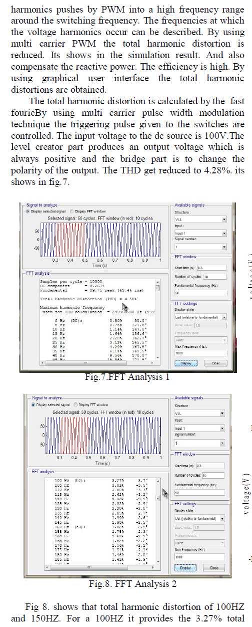
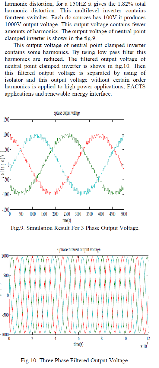
| The disturbances in power electronics equipment are often periodic and rich in higher harmonics. They have been frequencies and are often above the bandwidth of regulators used to control fundamental components. Therefore the ‘regular’ control can only partially reduce their effects on the distortion of control variables. This hysteresis control technique enables us to obtain better selective harmonic reduction in the output AC voltage. Finally, we obtained the output AC voltage waveform. Besides that, it realized better multilevel output and achieved desired results. Balance the voltage of the dc split capacitors of 15-L neutral point clamped inverter, and reduce the harmonics when multi carrier PWM modulation is employed. The total harmonic distortion is reduced to 4.58%.The number of level is increase in the Neutral point clamped multilevel inverter in order to reduce the selective harmonics elimination and to increase the voltage gain and power quality. |
References |
|