International Journal of Innovative Research in Science, Engineering and Technology
ISSN ONLINE(2319-8753)PRINT(2347-6710)
ISSN ONLINE(2319-8753)PRINT(2347-6710)
JansiRani.V 1, Rahila.J 2, Santhi.M3
|
| Related article at Pubmed, Scholar Google |
Visit for more related articles at International Journal of Innovative Research in Science, Engineering and Technology
In this present existing power scenario to meet out the demand multilevel inverter technology has emerged recently are very important alternative in the area of high power medium voltage applications. This paper proposes a trinary hybrid 81-level multilevel inverter for medium voltage applications. An 81 level inverter is designed to increase the quality of the output waveform to sinusoidal. Particularly, an 81-level inverter is an optimization in the number of levels for a given number of power transistors in power converters. The proposed topology uses reduced number of switching devices and thus reducing losses and low THD in comparison with the conventional topology. The configuration of the circuit is simple and easy to control. The operational principle and waveforms are illustrated and analyzed. To validate the proposed topology, the circuit is simulated and verified using Matlab /Simulink
Keywords |
| Hybrid multilevel inverter, minimum switches, trinary logic, 81- levels. |
INTRODUCTION |
| Multilevel inverter is originally developed for medium voltage drive of ac motor. As the number of voltage level increases, the output voltage waveform adds more steps and the output current waveform has lower total harmonic distortion. The advantages of multilevel inverters are higher voltage capability, reduction of input and output harmonic content, lower switching losses, higher amplitude fundamental and lower dv/dt. Another major advantage of multilevel inverter is that their switching frequency can be lower than the conventional two level inverter for the same THD of the output voltage, which means lower switching losses and increased efficiency [1], [2]. |
| At present there are three basic Multilevel inverters topologies; diode clamped (DCMI), flying-capacitor (FCMI), and multi module cascaded inverter (MMCI) [3]-[7].These are shown below in fig.1, fig.2, fig.3 [4]. For research on multilevel inverter topologies [4] a preferred multilevel inverter topology shall have the following characteristics. (1).The level is easy to extend (2).The number of the separated DC sources is few (3).There is no voltage balance problem (4).It has a modular structure. |
 |
| Fig.1.DCMI |
 |
| Fig.2.FCMI |
| A CMC [8] as shown in fig.3 is easy to design and easy packaging is also possible in CMC topology as each level has the same structure and there are no extra clamping diodes or voltage balancing capacitors [9], which are required in the DCMC and the FCMC. The number of output voltage levels can be easily adjusted by changing the number of full-bridge converters. The CMC synthesizes a desired voltage from the several independent DC voltage sources which may be obtained from batteries, fuel cells or solar cells. [10]. In general, the output voltage of CMC is controlled by [11]: |
| (1).By controlling the pulse width of the output voltage by fundamental frequency switching (FFS) method (or) PWM technique [12]-[14] while keeping the magnitude of dc voltage fixed. (2).By controlling the magnitude of dc voltage while keeping the pulse width of output voltage fixed or by controlling the Modulation index in case of PWM. (3). By controlling both the magnitude of dc voltage and the Pulse width of the output voltage. |
| The basis of selecting the method of controlling the converter output voltage is dependent on the ability to control the THD. The objective of achieving minimum THD [15]-[17] is based on two switching methods, the fundamental frequency switching (FFS) & multi-carrier based PWM technique. [18], FFS modulation [19], [20] can be easily implemented for the CMC due to its unique structure. All switching angles can be calculated off-line and then stored in a look-up table for digital implementation. |
 |
| Fig.3 cascaded H-bridge multilevel inverter |
| Compared with the carrier-based PWM schemes, FFS features low switching losses since all the IGBT switches operate at fundamental frequency. As the expressions for switching angles are nonlinear and transcendental, deriving a valid solution over the full range of amplitude modulation index (ma) [21] is not always possible. |
| In the proposed paper an 81 level multilevel inverter with trinary logic scheme is designed which reduces the number of switches. This topology reduces the cost and size of the inverter thus reducing the switching losses. It uses level shifted multi carrier modulation technique. This technique reduces the THD% which improves power quality. |
MULTILEVEL INVERTER TOPOLOGIES |
 |
| Fig.4. Basic unit of multilevel inverter. . |
| The basic unit of multilevel inverter in the conventional topology is shown in fig.4. The conventional topology consists of four switches in an H bridge unit. |
 |
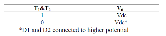
| TABLE I SWITCHING PATTERN-CONVENTIONAL TOPOLOGY |
| The Table I illustrates the switching scheme and output voltage for conventional topology. In the conventional topology, when T1 T2 is ON the output voltage is +VDC and when T3 T4 is ON the output voltage is –VDC. This topology permits the DC voltage sources to be distributed in equal, binary also in trinary pattern but number of switches is increased which increases the gate driver circuits. Switching losses are also increased. |
 |
| Fig.5. Multilevel inverter topology |
| In the topology presented above, each H-bridge module requires only two switches and the voltage levels can only be added which allows the input voltage to be distributed either equally or in binary pattern.(ie) Trinary distribution of DC sources is not possible with this configuration[23]. |
| For, |
| Equal DC source: Nstep = 2n +1, n = 1, 2, 3, (1) |
| BinaryDCsource: Nstep = n (n+1), n = 1, 2, 3,.. (2) |
| Where |
| n- Number of DC sources. |
 |
| Fig.6. Complementary switching circuit for 31 levels |
| In this circuit also Each H-bridge module requires only two switches. In the topology presented above also the voltage levels can only be added which allows the input voltage to be distributed either equally or in binary pattern. (i.e.) Trinary distribution of DC sources is not possible with this configuration [24]. |
| For |
| Binary DC source: Nlevel = 2(n + 1) m − 1. (3) |
| Where, |
| m – no. of stages in series |
| n - no. of dc sources |
PROPOSED MULTILEVEL INVERTER TOPOLOGY WITH MINIMUM NUMBER OF SWITCHES |
 |
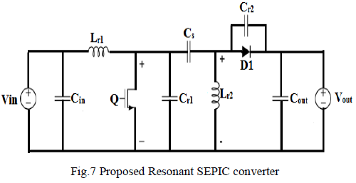
| Fig.7. Basic unit of proposed topology. |
| The basic unit of multilevel inverter in the proposed topology is shown in fig.7 respectively. The proposed topology consists of only two switches in an H-bridge unit. The proposed multilevel inverter requires bidirectional switches with the capability of blocking voltage and conducting current in both directions. Thus the number of switches is reduced to half which results in the reduction of gate driver circuits too. Therefore the control is made simple, easy and economic. Also the switching losses are reduced greatly. |
| TABLE II SWITCHING PATTERN-PROPOSED TOPOLOGY |
 |
| The Table II illustrates the switching scheme and output voltage proposed topology. In the proposed topology, whenT1 T2 is ON the output voltage is +VDC and when they are OFF the output voltage is - V DC, provided the diodes D1D2 are connected to higher potential. Thus, the proposed topology allows the DC voltage Sources to be distributed in trinary pattern. |
| For, |
| Equal DC source: Nstep = 2n +1, n = 1, 2, 3,.... (4) |
| Binary DC source: Nstep= 2 (n+1) - 1 n = 1, 2, 3. .. (5) |
| Trinary DC source: Nstep = 3n, n = 1, 2, 3 ... (6) |
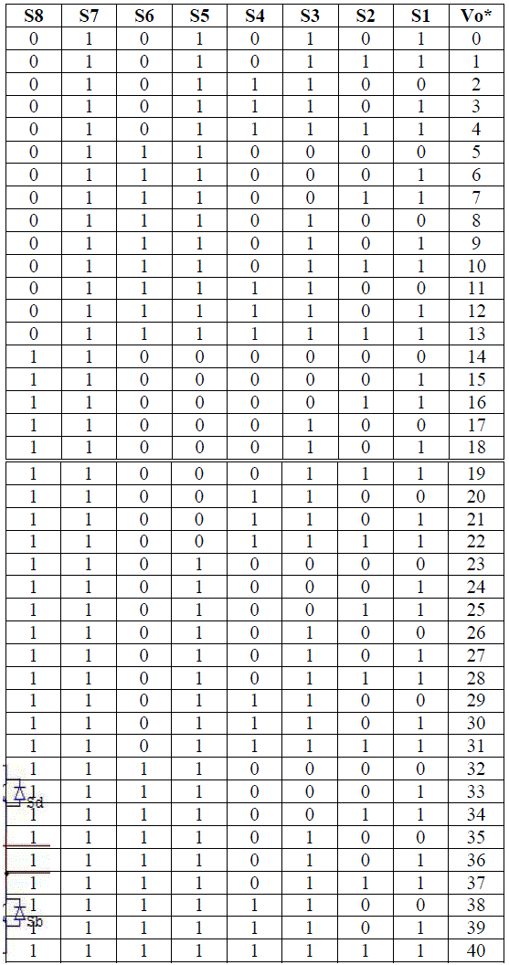
| The Fig.8 shows a basic idea to generate output voltage levels where VDCI = VDC, VDC2 =3VDC, VDC3 = 9VD C, VDC4 = 27V DC, The lower inverter generates a fundamental output voltage with nine levels, and then the upper inverters add or subtract one level from the fundamental wave to synthesize stepped waves. |
| The topology employs trinary dc input source. By using V DC, 3 V DC, 9V DC and 27V DC it can synthesize 81 output levels: -40VDC, -39VDC, -38VDC• · -VDC, 0, VDC •. . 39VDC, 40VDC as shown in Table III. |
 |
| Fig.8. Proposed topology for 81 levels. |
| TABLE III SWITCHING PATTERN-PROPOSED TOPOLOGY |
 |
MODULATION METHOD |
| When it comes to multilevel voltage source converters, the first notion is that need for a large number of switches that may lead to complex pulse-width modulation (PWM) switching scheme. However, early developments in this area demonstrated the relatively straightforward nature of multi level PWM [13]. Various PMW techniques applied to the multilevel converters are discussed in [12], [13] |
 |
| The most popular and simple switching scheme for multilevel voltage source converter is Multi-carrier- PWM (MCPWM) shown in Fig.9 (7 Level). For an NIevel converter, N-l carrier signals with the same frequency "fc" and peak-to-peak amplitude "Ac" are placed in such a way, that they occupy continuous bands between the positive and negative dc rail of the inverter [22]. The voltage reference or modulation waveform has peak-to-peak amplitude "Am" and frequency "fin", and it is centered in the middle of the carrier set. The voltage reference is continuously compared with each of the carrier signals. In multilevel converters, the amplitude modulation index (rna) and the frequency ratio (mf) are defined by (1) and (2), respectively. |
 |
 |
| There are three schemes for level shift multi-carrier modulation listed as follows: |
| 1) In-phase disposition (IPD): where all carriers are in phase. |
| 2) Alternative phase opposite disposition (APOD): where all carriers are alternatively in opposite disposition. |
| 3) Phase opposite disposition (POD): where all carriers above the zero reference are in phase but in opposition with those below the zero reference. |
| This paper addresses a novel Cascaded H bridge multilevel inverter which uses trinary dc input source and minimum switching devices. Therefore the control is made simple and easy. Furthermore, Mat Lab embedded function is written for Constant voltage and constant frequency operation. The operational principle and key waveforms are illustrated in detail. To verify the performance of the proposed multilevel inverter, computer-aided simulations are performed. |
COMPARISON OF PROPOSED TOPOLOGY WITH EXISTING TOPOLOGY. |
| In the Existing topology each H-bridge module requires only two switches and the voltage levels can only be added which allows the input voltage to be distributed either equally or in binary pattern where as in the proposed topology the trinary configuration has dc voltage sources that are scaled by the factor of three. This trinary configuration provides the maximum number of voltage levels with constant number of IGBTs. In the proposed topology, the voltage levels can be added and subtracted which allows the input voltage to be distributed either equally, binary or in trinary pattern. |
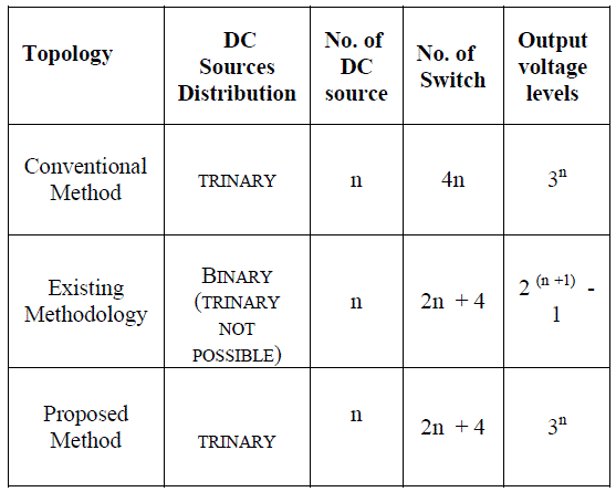 |
| TABLE-IV COMPARISON WITH RESPECT TO NO.OF SWITCHES, NO.OF SOURCES, NO.OF LEVELS |
 |
| Fig.10.Comparion of levels, switches, dc source for (a) conventional and proposed topology (b) reduced no. of switches and trinary proposed(c) complementary switching and trinary proposed |
SIMULATION RESULTS |
 |
| Fig.11. Output voltage and current waveform. Upper: Output voltage. Lower: Output current 100V/div, 2Aldiv and 0.01s/div. |
 |
| Fig.12. Voltage harmonics spectrum (81 Levels) |
| Fig 11 and Fig 12 represent the simulation result of output voltage, current and total harmonics distortion respectively. The synthesized output voltage waveforms for the above topologies show better output voltage quality and THD of 1.63%. |
 |
 |
| Fig.13.Input power Vs THD of 81 level trinary proposed MLI |
| EFFICIENCY CURVE |
 |
| Fig 14. Input power Vs Efficency of 81 level trinary proposed MLI |
CONCLUSIONS |
| A novel multilevel module (MLM) for the multilevel converter has been proposed. The proposed topology is a combination of MLMs and full-bridge converter. The proposed topology extends the design flexibility and the possibilities to optimize the converter for various objectives. It has been shown that the structure, consisting of MLMs with two switches has the minimum number of switches for a given number of voltage levels. The proposed topology has been compared with other topology. It has been shown that the proposed topology provides 81 levels on the output voltage using 12 IGBTs. But the topology presented in [24] produces only 31 voltage levels using 12 IGBTs. The proposed topology not only has lower switches and components in comparison with other one, but also it operates with trinary DC sources which increases the output voltage levels greatly as the number of multilevel modules increase. The proposed topology can be a good solution for applications that require high power quality, or applications that have considerable numbers of dc voltage sources. The operation and performance of the proposed topology has been verified through computer simulation. Analyses and simulations demonstrated the superiority of the proposed system. |
References |
|