International Journal of Innovative Research in Science, Engineering and Technology
ISSN ONLINE(2319-8753)PRINT(2347-6710)
ISSN ONLINE(2319-8753)PRINT(2347-6710)
Kanagavalli.M1 and Sukumar.P2
|
| Related article at Pubmed, Scholar Google |
Visit for more related articles at International Journal of Innovative Research in Science, Engineering and Technology
In Modern Trends the demand for memory has been increased tremendously. The searching operation of data in memory is the main problem that faces user. It increases power consumption and access time. Ternary content addressable memory performs high speed lookup operation but when compared with SRAMs, TCAMs have certain limitation such as low storage density, relatively slow access time, low scalability, complex circuitry, and are very expensive. Thus in this paper two works has been carried out, first one is TCAM uses the benefits of SRAM by configuring it (with additional logic) to enable it to behave like, it named as ZTCAM, which emulates the TCAM functionality with SRAM. SRAM is more faster and reliable memory. The static is derived from the fact that it doesn’t need to be refreshed. In the proposed ZTCAM hybrid partitioning of TCAM table is used, which partitioned the given data into many layer with low power. The proposed approach mainly user of SRAM read operations for comparisons. Second work has to be designing Asynchronous Transfer Mode (ATM) .Here Z-TCAM has been used in Asynchronous Transfer Mode (ATM) switching network components as a translation table. Here Z-TCAM architecture has been designed using SRAM, Flip-Flops and Asynchronous Transfer Mode has been designed with STT-RAM (Spin Transfer Torque), as compared with SRAM, the STT-RAM consumes less power. Z-TCAM has been successfully simulated using Tanner EDA and also designed using 0.18 μm technology.
Keywords |
| Application-specific integrated circuit (ASIC), Asynchronous Transfer Mode (ATM),Static random access memory (SRAM), Ternary content addressable memory (TCAM). |
INTRODUCTION |
| Z-TCAMs can be used in Asynchronous Transfer Mode (ATM) switching network components as a translation table. Since ATM networks are connection-oriented, virtual circuits need to be set up across them prior to any data transfer. There are two kinds of ATM virtual circuits: Virtual Path (identified by a virtual path identifier or VPI) and Channel Path (identified by a channel path identifier or VCI). VCI/VPI values are localized; each segment of the total connection has unique VPI/VCI combinations. Whenever an ATM cell travels through a switch, its VPI/VCI value has to be changed into the value used for the next segment of connection. This process is called VPI/VCI translation. Since speed is an important factor in ATM network, the speed at which this translation occurs forms a critical part of the networks overall performance.TCAM (ternary content-addressable memory) is a specialized type of high-speed memory that searches its entire contents in a single clock cycle. The term “ternary” refers to the memory's ability to store and query data using three different inputs: 0, 1 and X. The “X” input, which is often referred to as a “don’t care” or “wildcard” state, enables TCAM to perform broader searches based on pattern matching, as opposed to binary CAM, which performs exact-match searches using only 0s and 1s.TCAM is commonly found in networking equipment, such as high-performance routers and switches, to increase the speed of route look-up, packet classification. |
A. RELATED WORK |
| Summarize RAM-based solutions for CAM in this section. The methods proposed in [2] and [12] use hashing to build CAM from RAM but these methods suffer from collisions and bucket overflow. If many records have been placed in an overflow area, then a lookup may not finish until many buckets are searched. In [12], when stored keys contain don’t care bits in the bit positions used for hashing, then such keys must be duplicated in multiple buckets, which need increased capacity. On the other hand, if the search key contains don’t care bits which are taken by the hash function, multiple buckets must be accessed that results in performance degradation. The method proposed in [13] combines RAM and CAM to develop the CAM functionality. This approach makes partitions of the conventional TCAM table using some distinguishing bits in CAM entries. In NAND type CAM has been designed, in which XNOR gate is used to implement its design. In figure shows typical CAM cell of XNOR type. It is a compare unit of search operation. Here the compare unit, a pull-down transistor X, which is gate-controlled by the comparison result, is necessary to connect/disconnect the match line (ML) to/from the ground [1] The NAND-type CAM aims to reduce the power dissipated in search operation, in which the CAM cell is implemented as XNOR-type instead of XOR-type, and the pull-down transistors of each CAM cells are arranged in NAND type. However using match lines are very capacitive and consume much time for charging and discharging, so itconsumes more power. |
ARCHITECTURE OF Z-TCAM |
| Z-TCAM has a deterministic search performance that isindependent of data, efficiently handles the wild-cards, and has bettermemory utilization. Z-TCAM is generic and has aneasy partitioning scheme. ZTCAM supports an arbitrarily large bit pattern, considers the storage oforiginal addresses, while using appropriate partitioning. |
| A. Overall Architecture of Z-TCAM: The overall architecture of Z-TCAM is shown in Figure1, where each layer represents the architecture. It has L layers and a CAM priority encoder (CPE). Each layer outputs a potential match address (PMA). The PMAs are fed to CPE, which selects match address (MA) among PMAs. |
 |
| 1)Validation Memory: Size of each VM is 2w× 1 bits where W represents the number of bits in each sub-word and 2W shows the number of rows. A sub-word of W bits implies that it has total combinations of 2wwhere each combination represents a sub-word. For example, if W is of 4 bits, then it means that there are total of 24 = 16 combinations. This explanation is also related to OATAM and OAT. Each sub-word acts as an address to VM. If the memory location be invoked by a sub-word is high, it means that the input sub-word is present, otherwise absent. Thus, VM validates the input sub-word, if it is present. |
| 2) 1-Bit AND Operation: It performs the AND operation of the output of all VMs. The output of 1-bit AND operation decides the continuation of a search operation. If the result of 1-bit AND operation is high, then it permits the continuation of a search operation, otherwise mismatch occurs in the corresponding layer. |
| 3) Original Address Table Address Memory: Each OATAM is of 2w× w bits where 2wis the number of rows and each row has w bits. In OATAM, an address is stored at the memory location indexed by a sub-word and that address is then used to invoke a row from its corresponding OAT .If a sub-word in VM is mapped, then a corresponding address is also stored in OATAM at a memory location accessed by the sub-word. |
| 4) Original Address Table: Dimensions of OAT are 2w× K where w is the number of bits in a sub-word, 2wrepresents numberof rows, and K is the number of bits in each row where each bit represents an original address. Here K is a subset of originaladdresses from conventional TCAM table. It is OAT, which considers the storage of original addresses. |
| 5) K-Bit AND Operation: It ANDs bit-by-bit the read out K-bit rows from all OATs and forwards the result to LPE. If two inputs K-bit row from output of OATs then the output is high otherwise zero. |
| 6) Layer Priority Encoder: Because it emulate TCAM and multiple matches may occur in TCAM, the LPE selects PMA among the outputs of K-bit AND operation. |
| C. Hybrid Partitioning Of TCAM Table: Hybrid partitioning (HP) is a collective name given to vertical partitioning and horizontal partitioning of the conventional TCAM table. An example of HP is given in Table 1. HP partitions conventional TCAM table vertically (column wise) and horizontally (row wise) into TCAM sub-tables, which are then processed to be stored in their corresponding memory units. Vertical partitioning (VP) implies that a TCAM word of C bits is partitioned into N sub-words; each sub-word is of w bits. VP is used in Z-TCAM to decrease memory size as much as possible. Horizontal partitioning (HrP) divides each vertical partition using the original address range of conventional TCAM table into L horizontal partitions. |
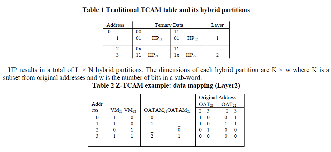 |
| Table 2 shows that sub-word 00, 01, and 11 are mapped in VM21. This states that memory locations 00, 01, and 11 should be high in VM21 and the remaining memory locations are set to low because their corresponding sub-words do not exist. And also, Table 2 shows OATAM21 where addresses are stored at the memory locations 00, 01, and 11. |
| D.Z-TCAM Operations: There are two types of ZTCAM operations to perform search operation such as data mapping, and data searching operation. In the data mapping operation the given dada is partitioned into two sub-words. The data searching operation described as algorithm1. |
| E. Data Mapping Operation: Classical TCAM table is logically partitioned into hybrid partitions. Each hybrid partition is then expanded into a binary version. Thus, first expand x into states 0 and 1 to be stored in SRAM. For example, if TCAM word of 010X, then it is expanded into 0100 and 0101. Each subword, acting as an address, is applied to its corresponding VM and logic ‘1’ is written at that memory location. |
| F. Search Operation: The searching operations are performed in two methods,searching in a layer of Z-TCAM and searching in ZTCAM. |
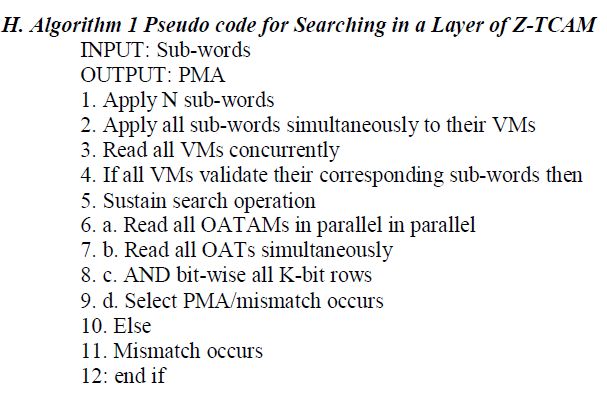
| G. Searching in a Layer of Z-TCAM: Algorithm 1 describes searching in a layer of Z-TCAM. N sub-words are concurrently applied to a layer. The sub-words then read out their corresponding memory locations from their respective VMs.Upon validation of all sub-words, the sub-words read out their respective memory locations from their corresponding OATAMs concurrently and output their corresponding OATAs. All OATAs then read out K-bit rows from their corresponding OATs simultaneously, which are then bitwise ANDed.LPE selects PMA from the result of the K-bit AND operation. |
 |
| I. Searching in Z-TCAM: Search operation in the proposed TCAM occurs concurrently in all layers, which follows Algorithm 2. Search key is applied to Z-TCAM, which is then divided into N sub-words. After searching, PMAs are available from all layers. CPE selects MA among PMAs; otherwise a mismatch of the input word occurs. |
J.Algorithm 2 Pseudo code for Searching in Z-TCAM |
| INPUT: Search Key |
| OUTPUT: MA |
| 1. Apply search key |
| 2. Divide search key into N sub-words |
| 3. All layer use algorithm 1 in parallel |
| 4. Select MA among PMAs/mismatch occurs |
Z-TCAM RESULT AND DISCUSSION |
A. Schematic diagram of Z-TCAM |
 |
| The Fig.3.shows the schematic diagram of ZTCAM .Here the circuit is designed with SRAM (2T SRAM). It emulates the TCAM functionality with SRAM. |
B. Simulation Output of Z-TCAM |
| The ZTCAM is simulated by using Tanner EDA software is shown in Figure 4. Here d1, d2, d3, d4 are the input signal and the output can be obtained in Out1, Out2.If given input data is 0011 means that the output will be the 00(from the table 1,in 0th address the data 0011is mapped . |
 |
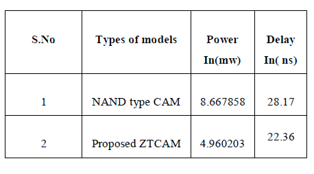
COMPARISON TABLE |
| Table 3 :Comparison result of SRAM based TCAM of ZTCAM and Conventional hybrid-type CAM ,in the first work NAND type CAM and Z-TCAM have been designed using SRAM and compared their power and delay. |
 |
ASYNCHRONOUS TRANSFER MODE (ATM) SWITCH DESIGN USING Z-TCAM |
| A. Asynchronous Transfer Mode (ATM) |
| Asynchronous Transfer Mode (ATM) is, according to the ATM Forum, "a telecommunications concept defined by ANSI and ITU (formerly CCITT) standards for carriage of a complete range of user traffic, including voice, data, and videosignals".ATM was developed to meet the needs of the Broadband Integrated Services Digital Network, as defined in the late 1980s, and designed to unify telecommunication and computer networks. It was designed for a network that must handle both traditional high-throughput data traffic (e.g., file transfers), and real-time, low-latency content such as voice and video. The reference model for ATM approximately maps to the three lowest layers of the ISO-OSI reference model: network layer, data link layer, and physical layer. ATM is a core protocol used over the SONET/SDH backbone of the public switched telephone network (PSTN) and Integrated Services Digital Network (ISDN), but its use is declining in favor of all IP.ATM provides functionality that is similar to both circuit switching and packet switching networks: ATM uses asynchronoustime-division multiplexing, and encodes data into small, fixed-sized packets (ISOOSI frames) called cells. This differs from approaches such as the Internet Protocol or Ethernet that use variable sized packets and frames. ATM uses a connection-oriented model in which a virtual circuit must be established between two endpoints before the actual data exchange begins. |
B. The structure of an ATM cell |
| An ATM cell consists of a 5-byte header and a 48-byte payload. The payload size of 48 bytes was chosen as described above.ATM defines two different cell formats: UNI (User-Network Interface) and NNI (Network-Network Interface). Most ATM links use UNI cell format. |
 |
| Single network connection, in the same way that two Integrated Services Digital Network (ISDN) phones can share a single basic rate ISDN connection. All four GFC bits must be zero by default.The NNI cell format replicates the UNI format almost exactly, except that the 4-bit GFC field is re-allocated to the VPI field, extending the VPI to 12 bits. |
ATM SWITCH DESIGN USING Z-TCAM |
| Z-TCAMs can be used in Asynchronous Transfer Mode (ATM) switching network components as a translation table. Since ATM networks are connection-oriented, virtual circuits need to be set up across them prior to any data transfer. There are two kinds of ATM virtual circuits: Virtual Path (identified by a virtual path identifier or VPI) and Channel Path (identified by a channel path identifier or VCI). VCI/VPI values are localized; each segment of the total connection has unique VPI/VCI combinations. Whenever an ATM cell travels through a switch, its VPI/VCI value has to be changed into the value used for the next segment of connection. This process is called VPI/VCI translation. Since speed is an important factor in ATM network, the speed at which this translation occurs forms a critical part of the network’s overall performance. |
 |
| Z-TCAM can act as an address translator in an ATM switch and perform the VPI/VCI translation very quickly. During the translation process, the Z-TCAM takes incoming VPI/VCI values in ATM cell headers and generates addresses that access data in an external RAM (since standard CAM architectures cannot support the required capacity, a CAM/RAM combination enables the realization of multi- megabit translation tables with fully-parallel search capability). VPI/VCI fields from the ATM cell header are compared against a list of current connections stored in the CAM array. As a result of the comparison, CAM generates an address that is used to access an external RAM where VPI/VCI mapping data and other connection information is stored. The ATM controller modifies the cell header using the VPI/VCI data from the RAM, and the cell is sent to the switch. |
SPIN TRANSFER TORQUE RANDOM ACCESS MEMORY (STT-RAM) |
| Spin transfer torque random access memory (STT-RAM) is an emerging memory technology that promises to deliver the benefits of current non-volatile memories (speed, high density) with the added benefit of being non-volatile and offering no leakage power from the storage element. |
 |
| However, before these benefits can be reaped, memory designers (both architects and circuit designers) must be able make Informed design decisions to meet specific application needs while minimizing unwanted effects. |
RESULT AND DISCUSSION OF ATM SWITCH |
A. Schematic diagram of ATMswitch |
| The Fig.8.shows the schematic diagram of ATM Switch.Here the circuit is designed with STT-RAM (2T SRAM). Its output is corresponding to the Z-TCAM. |
 |
CONCLUSION |
| In this project, SRAM based TCAM architecture of Z-TCAM and ATM switch has been proposed, it ensures large capacity TCAM whereas this capability is lacked by conventional ones. Moreover, the proposed TCAM has a simpler structure, and very importantly, has a deterministic search performance of one word comparison per clock cycle and using SRAM. The searching operation of proposed system has been designed using SRAM. SRAM devices are denser, cheaper, and operate faster than TCAM devices. Here ATM Switch has been designed using SST-RAM and Z-TCAM used as a component; it can be performed in ATM Switch as a translation table. As compared with SRAM, the STT-RAM consumes less power and delay in data searching operation. The power and delay overhead of the proposed scheme is simulated using TANNER EDA. |
References |
|