International Journal of Innovative Research in Science, Engineering and Technology
ISSN ONLINE(2319-8753)PRINT(2347-6710)
ISSN ONLINE(2319-8753)PRINT(2347-6710)
| A.G. Karthikeyan, P. Sathyanathan, S. Saravanan and M. Vimala Department of Electrical and Electronics Engineering, Magna College of Engineering, Chennai, India |
| Related article at Pubmed, Scholar Google |
Visit for more related articles at International Journal of Innovative Research in Science, Engineering and Technology
this paper proposes a new multi-level inverter topology based on a H-bridge structure with four switches connected to the dc-link. Based on a POD (Phase opposition disposition) modulation method, a new PWM method which requires only one carrier signal is suggested. The switching sequence to balance the capacitor voltage is also considered. In addition to these, the proposed topology requires minimum number of component count to increase the number of voltage level. Operating principle of the proposed inverter is verified through simulation and experiment.
INTRODUCTION |
| Due to the increasing demand on the renewable energy sources, grid connected inverter systems are becoming more and more important than ever before. For grid connected operation, the inverter should meet the following requirements. |
| 1. The inverter has to generate a pure sinusoidal output voltage. |
| 2. The inverter output current should have low total harmonic distortion (THD). |
| Traditionally, two-level PWM inverter is used for grid-tied operation. In case of a two-level inverter, the switching frequency should be high or the inductance of the output filter inductor need to be big enough to satisfy the required THD. To cope with the problems associated with the two-level inverter, multi-level inverters (MLIs) are introduced for gridconnected inverter. Several MLI topologies have been suggested so far and they can be mainly classified as three types in Fig. 1; neutral point clamped (NPC), flying capacitor (FC), and cascaded type [3-5]. |
| Advantage of the MLIs is that their switching frequency and device voltage rating can be much lower than those of a traditional two-level inverter for the same output voltage. Therefore, IGBT switching loss can be reduced significantly and thus the inverter system efficiency can be increased [6-8]. |
| In this paper, a circuit based on a H-bridge topology with four switches connected to the dc-link is proposed as a MLI topology. Fig. 2 shows the proposed MLI. Also it is simple because the proposed PWM method uses one carrier signal for generating PWM signals. In addition, the switching sequence considering the voltage balance of dc-link was proposed. Finally, the proposed topology of the multi-level inverter is verified by showing the feasibility through the simulation and the experiment. |
 |
| Figure 1: Topologies of multi-level inverters. (a) neutral point clamped (NPC) type. (b) Flying capacitor (FC) type. (c) Cascade type. |
PROPOSED MULTI-LEVEL INVERTER |
| A.Topology of multi-level inverter |
 |
 |
| B.Operating modes and proposed PWM strategy |
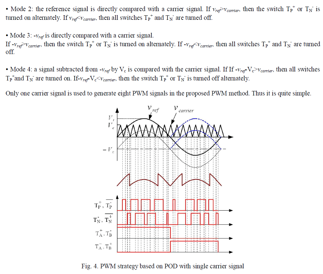
| The output voltage of the proposed MLI shown in Fig. 2 has five levels (VDC, VDC/2, 0, -VDC/2, -VDC) according to the switching states of the inverter. There are four operation modes depending on the instantaneous value of the reference voltage, vrefand the maximum value of the carrier signal, VC(see Fig. 4). Table II shows the possible inverter output voltage level according to the operating mode. |
| In case of the N-level NPC type multi-level inverter, N-1 triangular carrier signals with the same frequency and amplitude are used so that they fully occupy contiguous bands over the range +VDC to -VDC. A single sinusoidal reference is compared with each carrier signalto determine the output voltage for the inverter. Three dispositions of the carrier signal are considered to generate the PWM signal [9-11]. |
| 1) Phase disposition (PD); where all carriers are in phase. |
| 2) Alternative phase opposition disposition (APOD); where each carrier is phase shifted by 180 degree from its adjacent carrier. |
| 3) Phase opposition disposition (POD); where the carriers above zero voltage are 180 degree out of phase with those below zero voltage. |
| Fig. 3 shows the reference signal and the carrier signal arrangements for PD modulation, POD modulation, and APOD modulation. |
| A new PWM strategy based on POD modulation which requires only a single carrier signal (vcarrier) is proposed and the detailed PWM strategy is depicted in Fig. 4. If the |
 |
| Figure 3: Carrier and reference signal arrangements for: (a) Phase disposition (PD). (b) Alternative phase opposition disposition (APOD). (c) Phase opposition disposition (POD). |
| reference signal is positive, then the switch pair (TA +, TB-) are turned on, and if it is negative, then the switch pair (TA-, TB+) are turned on. Thus the switches composing the H bridge inverter turned on and turned off once during the period of the reference signal. The voltage across the switch at blocking state is VDC. The switches (TP -, TN +) are operated complementally to the switches (TP +, TN -). The generation of the PWM signal for dc-link switches (TP +, TN -) can be explained as follows. |
| • Mode 1: a signal subtracted from the reference signal by |
 |
| C.Voltage balancing of dc-link capacitor |
| One of the important issues about multi-level inverter is the voltage balance of the dc-link capacitor. The voltage of capacitor C1 and C2 should be equally balanced to VDC/2. However the midpoint voltage fluctuates when C1 and C2 charge and discharge continuously. If the capacitor voltage is unbalanced, the output voltage becomes unsymmetrical and it results in a high harmonic content in the load current. |
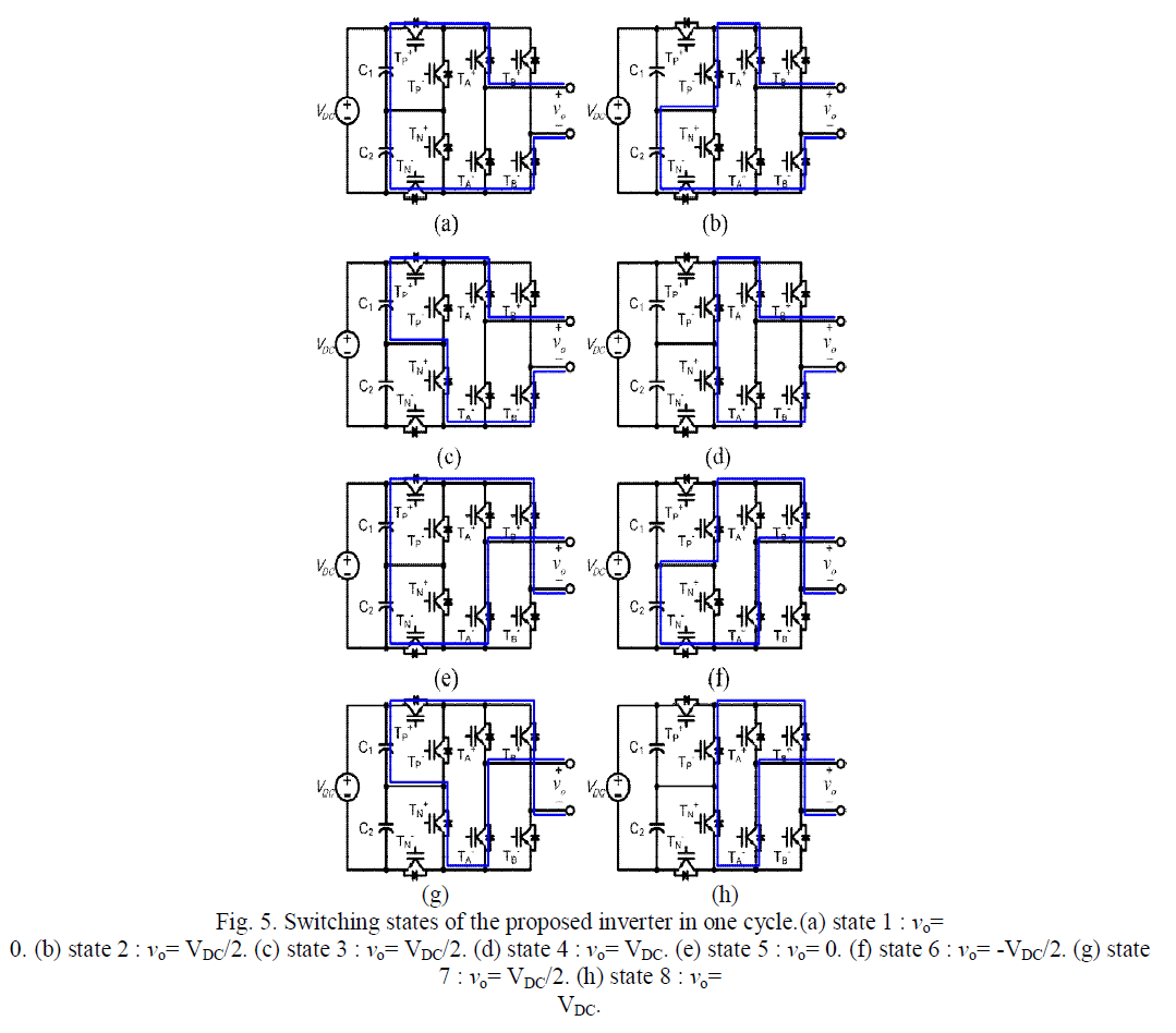
| To solve this problem, the switching state should be selected appropriately in Fig. 5. If only one switch in a dc- link is turned on, the output voltage becomes VDC/2. In order to balance the voltage of dc-link capacitor, dc-link switches (TP +, TN -) are alternately turned on at mode 2, and alternately turned off at mode 1. And switches (TP -, TN +) are operated complementally to switches (TP +, TN -). Therefore, the switching sequence of mode 1 is (a)-(b)-(a)-(c), and the switching sequence of mode 2 is (d)-(b)-(d)-(c). The switching sequence of mode 3 and mode 4 are similar that of mode 1 and mode 2. The switching sequence of mode 3 is (h)-(f)-(h)(g), and the switching sequence of mode 4 is (e)-(f)-(e)-(g). |
 |
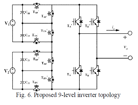 |
| D.Extension to 9-level inverter |
| It should be noted that although the number of the switching devices in the proposed 5-level inverter (shown in Fig. 2) is the same as that of the conventional cascaded H-bridge MLI, the switches (TA +, TA-, TB+, TB-) in the proposed MLI are switched at a low frequency(60 Hz). Moreover, unlike the cascaded H-bridge MLI, the proposed 5-level inverter requires only one isolated voltage source, VDC. |
| In order to maximize the effectiveness of the proposed MLI, 9-level inverter which was extended from 5-level inverter shown in Fig. 2 is also proposed in this paper and the overall circuit diagram is shown in Fig. 6. As shown in Fig. 6, in case of 9-level inverter, the proposed inverter requires less active devices than 9-level cascaded H-bridge MLI. Therefore, number of switching devices in the proposed MLI can be reduced significantly as the number of voltage level increases. |
SIMULATION AND EXPERIMENTAL RESULTS |
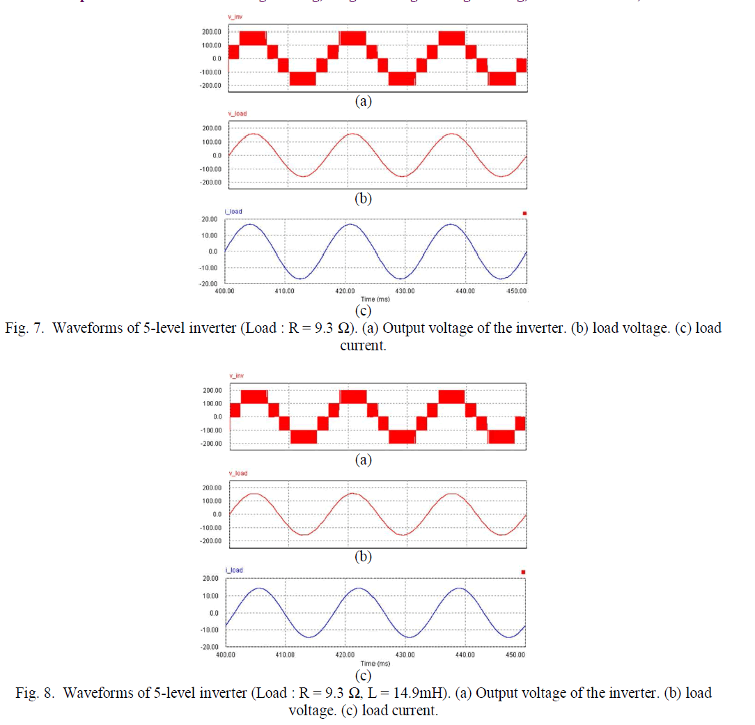
| The proposed 5-level inverter is tested to verify the operating principle of the proposed MLI. The LC filter is inserted between the output of the inverter and the load. Electrical specifications of the proposed inverter are summarized in Table III. Fig. 7 and 8 show simulation waveforms of the proposed inverter in 5-level. Fig. 7 shows the waveforms of the inverter output voltage, load voltage and the load current when the power factor becomes unity. Fig. 8 shows the waveforms of the inverter output voltage, load voltage and the load current during the lagging power factor. |
 |
 |
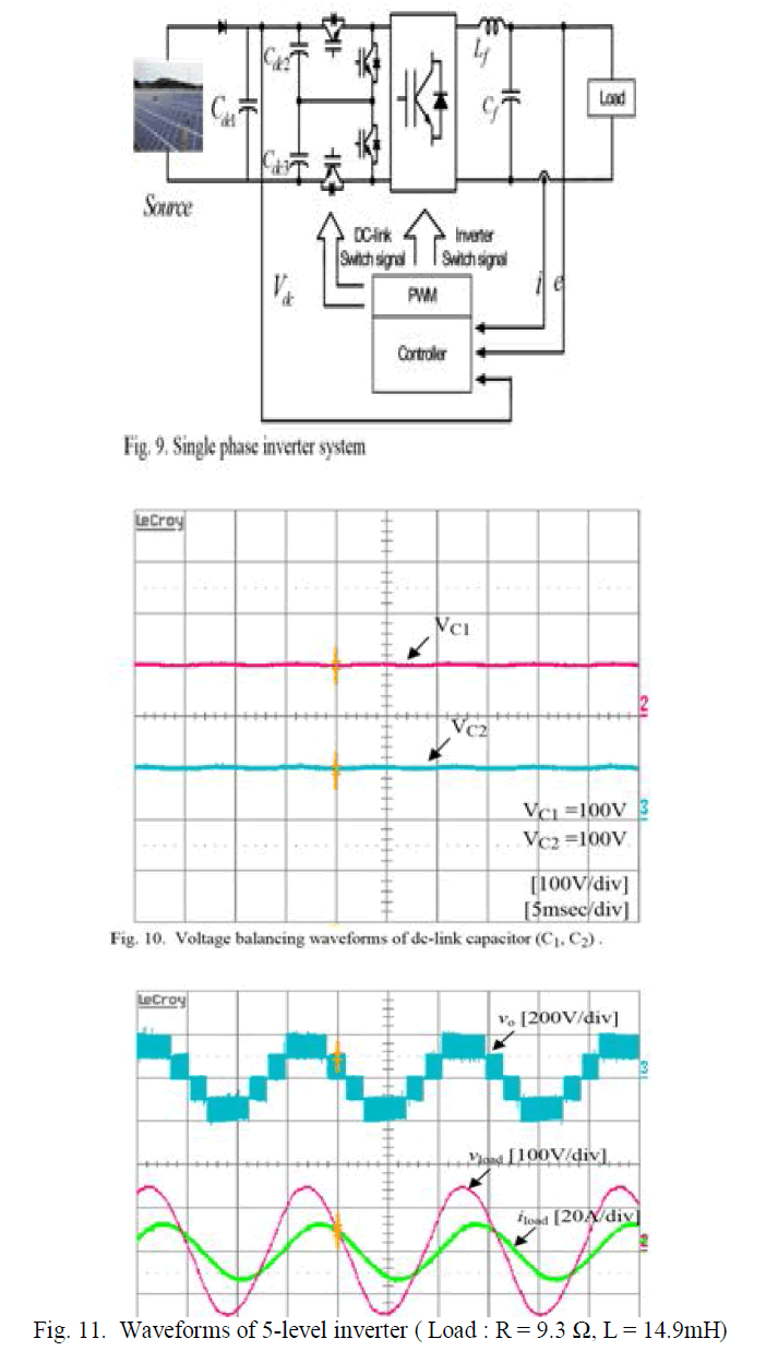
| Based on the simulation results, the experiment was conducted. Rating and the parameters of the system which was used in the experiment are the same with those of the simulation. Configuration for the experiment is shown in Fig. 9. Fig. 10 shows that the capacitor voltages (VC1, VC2) are controlled constantly. The capacitor voltages (VC1, VC2) are well balanced at the voltage of 100[V]. Fig. 11 shows the waveforms of the inverter output voltage, load voltage and the load current. The inverter output voltage is 5-level voltage and the load current and the load voltage waveforms are closer to the sinusoidal waveform. Experimental output waveforms can be found consistent with the simulation result. |
 |
CONCLUSION |
| This paper proposed a new multi-level inverter topology based on a H-bridge inverter with four switches connected to the dc-link. The proposed MLI has the following advantages over the conventional inverters. |
| 1. Number of devices of the proposed multi-level inverter is fewer than that of the conventional multi-level inverters. Therefore, the proposed system is more reliable and cost competitive than the conventional two-level and multilevel inverters. |
| 2. The four switches (TA +, TA-, TB+, TB-) in the H-bridge are switched at a low frequency (e.g. 60 Hz). Therefore, switching loss of The four switches (TA +, TA-, TB+, TB-) is almost negligible. |
| 3. Only one carrier signal is required to generate the PWM signals for 4 switching devices (TP +, TP -, TN +, TN -). |
| 4. The proposed topology can be easily extended to 9-level or higher level with minimized active device component count. |
ACKNOWLEDGMENT |
| This work was supported by the Power Generation & Electricity Delivery of the Korea Institute of Energy Technology Evaluation and Planning (KETEP) grant funded by the Korea government Ministry of Knowledge Economy (No. 20111020400260) |
References |
|