International Journal of Innovative Research in Science, Engineering and Technology
ISSN ONLINE(2319-8753)PRINT(2347-6710)
ISSN ONLINE(2319-8753)PRINT(2347-6710)
S.Sridevi1, G.Muralidharan2, C.Nandha kumar3
|
| Related article at Pubmed, Scholar Google |
Visit for more related articles at International Journal of Innovative Research in Science, Engineering and Technology
Discrete wired connections can be reduced in size into printed circuit board (PCB). PCB manufacturing involves various steps such as patterning, etching, drilling, masking and legend printing. During the manufacturing process of PCB hardware, the short circuits between tracks and pads, discontinuity of track and various defects may occur. This paper presents a novel technique for identification of such defects using machine vision and image processing techniques. This system reduces the time of inspection and increases the accuracy, even though the image scale varies with respect to the reference image. The constant stand of distance between the camera and PCB need not be maintained. The result of applying this technique into PCB layout and real images are shown.
Keywords |
| PCB inspection, Scale variant, Machine Vision, short circuited, tracks cuts. |
INTRODUCTION |
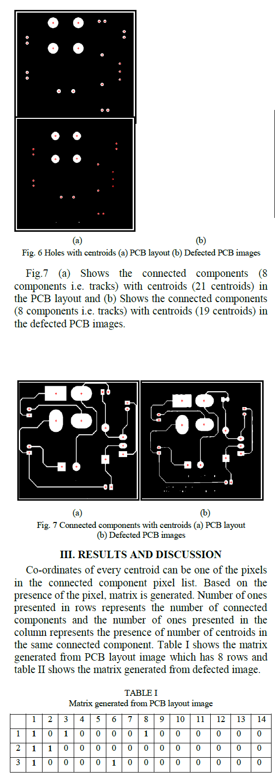
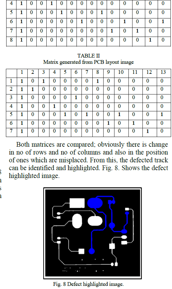
| connected table of a reference and a test image which described the method and its implementation of standard morphology image processing techniques [1]. To eliminate or to reduce the noise during the processing of defect identification, point to point image subtraction is used. Positive and negative images are generated and noise removal process is applied separately [2].To detect the defect presented in the PCB inner layers, fuzzy reasoning concept can be used. Image preprocessing is implemented to reduce the noise presented in the image. Image subtraction and boundary analysis techniques are applied to identify the defects [3].During image processing, misclassification error occurs, which can be reduced by evaluating the performance of thresholding algorithms. In this method, wrongly assigned pixels can be identified and filtered by choosing best thresholding algorithm [4]. Patterning is the initial process of PCB manufacturing. While patterning the PCB, images are captured using proper light settings. Image subtraction can be performed and defect can be identified [5]. Template is generated from the non-defected PCB and the template matching is performed with the defected PCB. So this defect can be identified. Missing and misaligned components are also inspected before the electronic test of the assembled PCB. The above nondestructive tests are performed and the defects are identified without any power supply given to the assembled PCB [6]. Machine vision is one of the advanced techniques which can explain about various lighting techniques for various applications, interfacing and data communication of various frame grabbers, industrial camera systems, lenses, camera calibration, and optical systems. Various lighting techniques are used to capture the image which is chosen based on the application. Front lighting is used to know about the surface information presented in the image. Back lighting is used to get the profile information presented in the image. It describes about various data cables with standard connectors. This work describes the reference image which is developed from the PCB layout file, the lighting technique which is used to acquire the PCB image, various noise reduction techniques using structuring elements, 2-D order-statistic filters and image processing algorithms to identify the short circuit between the tracks, pads and track cuts. For this purpose, numbers of connected components are used to identify the number of individual connections. Holes are separated and centroids are found from the holes presented in the acquired image and pixel list of connected components are sorted and checked whether the centroids are presented in the pixel list. Based on the connectivity result of the above steps, a connectivity matrix is generated for both PCB layout image and captured image. Both matrices are compared to identify the track short or track cut. |
METHODOLOGY |
 |
 |
 |
 |
CONCLUSION |
| For online inspection of PCB, a novel algorithm has proposed and implemented using machine vision and image processing techniques. The algorithm has discussed in detail and the result is shown. In spite the scale of images is varied, this method increases the accuracy of the inspection at a fast manner. To implement this algorithm in an industrial application, some automated systems need to be carried out. Future work consists of inspecting the assembled PCB for missing and misaligned components. |
ACKNOWLEDGEMENT |
| The authors would like to thank Assistant Professor R.Senthilnathan, Mechatronics, SRM University for his continuous moral support throughout this work. |
References |
|