International Journal of Innovative Research in Science, Engineering and Technology
ISSN ONLINE(2319-8753)PRINT(2347-6710)
ISSN ONLINE(2319-8753)PRINT(2347-6710)
RenuSahu1, Zoonubiya Ali2 and BalramTimande3
|
| Related article at Pubmed, Scholar Google |
Visit for more related articles at International Journal of Innovative Research in Science, Engineering and Technology
This study presents different structure of operational transconductance amplifier (OTA) which is an integral part of continuous time channel selection filter. It was observed that to enhance the linearity and to reduce the third order harmonic distortion, linearity schemes are used however most of those techniques present important drawback such as reduced effective transconductance, significant power consumption, limited frequency response, increased noise level. It presents new linearity scheme source degeneration and auxiliary differential pair technique by which the linearity can be increased without sacrificing other important parameters such as noise level, power efficiency and frequency response which is better than other schemes.
Keywords |
| CMOS analog circuits, operational transconductance amplifier (OTA), direct conversion receiver, transconductor, linearity schemes, continuous time filters. |
INTRODUCTION |
| High-performance filter is one the most important building block in analog domain for several applications such as read/write channels for hard-disk drivers, intermediate-frequency (IF) filtering for high speed wireless and wired communication systems and adaptive systems as reported in [1]-[12]. In receivers, before the subsequent analog to digital conversion stage, very demanding high performance analogue filters are typically used to block interferers and provide anti alias filtering. Sun Y. et al[13] reported that to design analogue filters with low power consumption and wide tuning range is very challenging. |
| A. Filter Basics |
| Filter is defined as the electric network which passes or allows unattenuated transmission of electric signal within certain frequency range and stops or disallows transmission of electric signal outside this range. |
| B. Types of filter |
| LacanetteetKerry al [14] presented the filters categorization based on the signals used, based on the components used, based on the frequency response and based on the mathematical functions. All these categorize are divided into subcategory. Signals based filters are divided into digital filters and analog filters, component based filters are divided into switched capacitor filters and active filters, frequency response based filters divided into low pass filters, high pass filters, band pass filters, band stop filters, all pass filters, mathematical functions based filters divided into Butterworth filters, Chebyshev filters and elliptic filters. |
| Gratz Achimet al [15] mentioned that the operational transconductance amplifier(OTA) has differential input voltage which produces an output current. Thus, it is a voltage controlled current source (VCCS). Also Geiger R. L. et al [16] presented basic structures using the transconductance amplifier. |
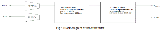
| For direct conversion receiver (DCR) application, wireless applications Butterworth, Elliptic and Chebyshev filters are mostly used.The main objective of this paper is to study the different order Butterworth filter. Also a design technique is presented to enhance the Butterworth filter performance based on OTA. |
BUTTERWORTH FILTER |
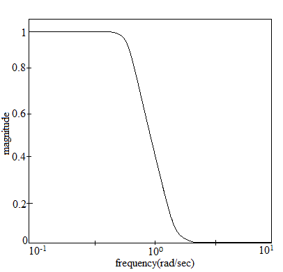
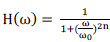
| Butterworth filter is suitable for applications in which any ripples are intolerable and also have a monotonic amplitude frequency response. Butterworth filter is characterized by having a maximally flat magnitude response for this reason; the Butterworth filter is also called a “maximally-flat magnitude” filters. The equation for Butterworth filter’s magnitude response is shown in fig 1 |
 |
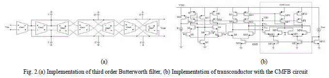
| a) OTA structure for 3rd order filter |
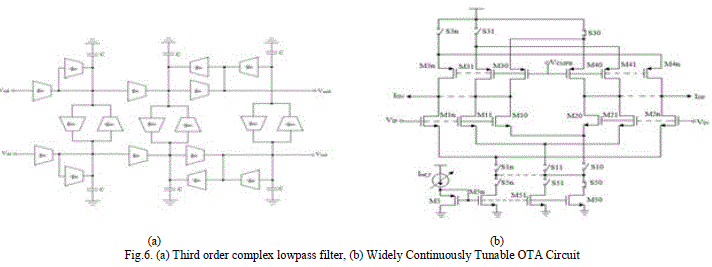
| The voltage-to-current (OTA) circuit as shown in fig 2(b) is based on flipped follower circuit (FLF) [17], which is composed by transistors M5 and M6. M1 and M2 transistor provides voltage to current conversion. The gate voltage of transistor M5 is used to provide a bias voltage for transistors M3 and M4, and ensure the linear region operation of transistors M1 and M2. Thus, the drain voltage of transistors M1 and M2 would be kept to a constant value. Input transistors operate in linear region. Besides, the source of transistors M1 and M2 is fixed to a constant value owing to the FVF feedback loop. Low impedance is obtained at the source of transistor M6.The structure suppresses the variation at the source of transistors M1 and M2, and thus the circuit would operate under a class-AB fashion. A common mode feedback (CMFB) circuit is required to control the output common-mode voltage. The output voltage of the transconductor is sensed by transistor MF3 and MF6, and then compared with a reference voltage, which is equal to the input common-mode voltage this input voltage owing to the cascade design of the filter structure. If common mode voltage is not equal to the reference voltage, a corrected current is mirrored by transistor MF9 to the load of the Transconductor, then the output Vcmis adjusted to the desired voltage. The aspect ratio of transistor M19 would be twice the value of transistors MF1 and MF2.This filter was simulated using 0.18μm CMOS technology provides tuning range 135 KHz - 2.2 MHz consuming power of 1.57 mw - 1.9mw. |
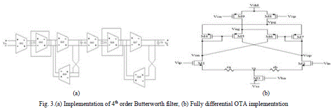
| B.Fourth Order Butterworth Filter |
| The fully differential transconductor-capacitor filter is shown in fig 3(a) by using two biquadratic sections fourth-order Butterworth is realized. Each biquad is implemented with 4 OTAs and 2 capacitors. The fully differential transconductor filter is shown in fig 3 (b) [18]a common mode feedback circuit (CMFB) is needed due to the fully differential circuit to set the DC output level of the filter. By varying the current through theOTAs in a range of 1:10 a tuning range of the corner frequency of about 1:3 can be achieved. |
| a) OTA structure for 4th order filter |
| In Fig. 3(b) the differential transconductance circuit is comprises a cross-coupled high-impedance load and a source-Coupled pair with poly-silicon degeneration resistors.The linearity is enhanced by the degenerated resistors at the cost of a smaller effective transconductanceGm and a smaller tunable Gm range. Transistors M8 and M9 operate in the triode region, acting as degeneration resistors to provide different operating points at nodes vpg and vng and transistors M4, M5, M6 and M7 are matched. M4 and M7 act like a pair of positive resistors R+, while M5 and M6 function as negative resistors R-. The output impedance of the transconductor depends on the parallel combination of R+ and R-, which are controlled by voltages vcp and vcn respectively. As a result, the output impedance, and therefore, the Q of the integrator, can be maximized with proper combinations of vcp and vcn. With this transconductor, a tunable integrator for very-high-frequency integrated filters can be realized by adjusting the voltage vba, which controls the tail current, and thus, Gm. Good high-speed properties stem from the absence of internal high impedance nodes, which, pushes non-dominant poles to the gigahertz ranges [18]. This filter was designed in 0.18μm CMOS technology provides tuning range from 1.4 MHz – 16 MHz |
 |
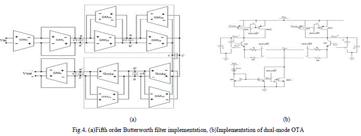
| C. Fifth Order Butterworth Filter |
| The fifth-order OTA-C filter is shown in fig 4(a) [19]the overall circuit is composed of two gyrators A and B, which implement the equivalent inductors L2and L4 respectively, two grounded resistors Gm0and Gm6 and five capacitors C1-C5. Five common-mode feedback circuit shared by eleven OTA’s reduces power consumption. The common mode feedback circuit provide sensing of common output voltages on nodes a to control the bias voltage vb3 of the OTA. |
| a) OTA structure for 5th order filter |
| The OTA-C structure for 5th order lowpass filter shown in fig 4 (b) was implemented with the two cascaded biquadratic sections. The OTA used source degenerated transconductance with current scaling. It enhances the limited linear input range of the bipolar differential pair. This circuit was simulated in 0.25μm CMOS technology tunable from 600 KHz – 6 MHz with current consumption of 0.9 -2.7 μA. |
 |
| transconductor to keep the CMFB loopstable. An automatic frequency tuning scheme is used to compensate for process variation [20] – [26]. In the OTA C filter shown in fig. 6(a) frequency tuning is achieved by tuning the transconductors with digital control signals.This filter was simulated in 0.18μm CMOS technology with tuning range 3 – 24 MHz |
 |
PROPOSED FILTER STRUCTURE |
| A circuit realization for the second order filter is used because of its advantages in design and layout. The topology of the fully differential circuit block is shown in fig 7(a) the transfer function of the above circuit structure is [27] |
 |
OTA DESIGN |
| Fig. 7(b) shows the complete diagram of OTA including the CMFB circuit. The transconductor core consist of a source degenerated differential pair with auxilliary differential techniqiue is presented. |
 |
 |
| OTA’s linearity improves by increasing Nr according to (5), but (6) shows that this approach will increase the input referred noise level, because the two tail current transistor introduce some differential noise if the value of source degenerated resistors is large, by placing the tail current transistor in the middle of the source degeneration resistor as shown in Fig. 8(c),This term can be minimized and the noise of the tail current split equally in both branches and appears as common mode noise which is rejected due to fully differential nature of the topology and the common node is always unaffected by the differential signal variations by using this topology. The drawback of the circuit shown in Fig. 8(c)is that the additional dc voltage drop through the degeneration resistors, thereby consuming voltage headroom for the input signal. Therefore limited overdriving voltages and source degeneration factor Nr must be used. |
| B. Auxiliary differential pair technique |
| In order to reduce the harmonic distortion components without sacrificing other parametersauxiliary differential pair technique is present in this pair. |
| To illustrate the concept, let us consider several differential pairs with its own degeneration resistor; the transconductance curves for fixedDegeneration resistances and curves for variable degeneration resistance with input voltage are plotted in Fig. 9(a), By using Auxiliary differential pair technique results in a flattened transconductance curve and enhanced linearity, therefore degenerated resistor is replaced by the parallel of a degenerated resistor and ADP shown in Fig. 9(b), Based on the current to voltage relation depicted in (1) for the differential pair of Fig. 8(a), the output current of the circuit in Fig. 9(b) written as |
 |
 |
| The proposed diagram of OTA including the CMFB circuit, tansistors MN1 use an overdrive voltage and the tail current flowing through MN3 i.e. tail current transistor, use of folded cascoding or any other additional circuit has been avoided the output is taken directly from the drains of MN1 which optimize the structure for power and noise performances. Transistors MN1 remain in saturation for output peak voltages of less than one half the threshold voltage of MN1, which is the case for the signals used in the filters implementation. For better transistormatching, all transistors lengths are equal except transistors MP3 to enhance the OTA output impedance. The CMFB circuit is designed with a power consumption of ¼ that of the core. By using these two techniques the circuit area reduces thus we can use this in wireless application such asmobile application as GSM, Bluetooth, and WCDMA etc. to meet the required specification. |
COMPARISON |
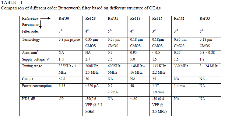
| TABLE – I |
| Comparison of different order Butterworth filter based on different structure of OTAs |
 |
RESULTS AND DISCUSSION |
| Results obtained from present study is summarized as: a) wide tuning range and high linearity can be achieved using better linearization technique to design operational transconductance amplifier(OTA). b) Low power consumption and small filter area can be easily optimized using lower order filter to fulfill the application requirement. |
| Filter is a very small element throughout the communication system, thus smaller filter area and low power consumption is required. Higher order filters provide wide tuning range and high linearity. Besides this higher order filterresults in increase power consumption and increased filter area because they have the large number of component.All these parameters can be achieved using two linearization techniques; source degeneration and auxiliary differential pair to design operational transconductance amplifier (OTA) and using lower order filter. |
CONCLUSION |
| The study of different filter orders has been carried out. Thereafter it is concluded that the increment in filterorder i.e. making higher order filter, leads the increment in the filter components. This is resulting in cost and area enhancement and also the design becomes complex. To optimize the complexity of structure, cost and area the best possible solution is to use the lower order filterwith OTA. The OTA is composed of two techniques which enhances the linearity of filter and does not affect other parameters and this gives wide tuning range with lower order filter. |
References |
|