Switched Boost Inverter (SBI) is a single stage DC to AC power converter and it is derived from the Z - source inverter employs an LC impedance network in between the main inverter bridge and the power source. This SBI converter can possible to supply both DC and AC loads simultaneously from a single dc input source. Here, reducing the inverter switching stress. Also, this converter provides to shoot- through of the inverter legs without causing any damage to the inverter switches. The unique feature of the SBI, it can operate either in buck or boost mode operations with a wide range of obtainable output voltages from a given input voltage, unlike the traditional buck-type voltage source inverter.SBI construct similar advantages of converter uses more switching devices and lower number of passive devices compared to the original ZSI. Along with its pulse width modulation (PWM) control strategies is give the inverter switching pulse. These features make the SBI suitable for variable motor speed drive application. The SBI reduce the electromagnetic interference noise immunity when compared to the VSI. which enables the compact design of the power converter.Here BLDC motor drive is using as a DC load and AC load as resistive load and non linear load.The theoretical and modulation concepts presented have been verified in simulation .The operating modes of the proposed converter are simulated using MATLAB.
Index Terms |
| pulse width modulation (PWM), switched
boost inverter (SBI), AC and DC Loads |
INTRODUCTION |
| This novel power converter called Switched Boost
Inverter (SBI) which works similarly to a Z-source
inverter, this topology construct similar properties of a
ZSI with minimum number of passive components and
many active components. This section presents a review
of the approach used to derive the SBI from IWJ topology
[11]. The ZSI consists of an X-shaped passive network to couple the main power converter and the power sources.
Unlike a traditional VSI [2],[3].the ZSI has the advantage
of either stepping up or stepping down the input voltage
by properly used the shoot-through state of the inverter
bridge which is achieved by allowing the shoot-through of
the inverter leg switches. As per the consumer prefers
each DC load and AC load in the application also has its
own power electronic interface for simplicity. |
| The application of motor speed control is based on the
proposed structure of SBI. The operating principle and
Pulse Width Modulation (PWM) control of the SBI has
been explained that SBI is a single-stage power converter.
That can supply both DC and AC loads simultaneously
from a single DC input. So, it can realize both the DC to
DC converter and the DC to AC converter in a single
stage. So, it has a wide range of obtainable output voltage
for a given source voltage. |
 |
| Switched boost inverter has exhibits better Electro
Magnetic interferences (EMI) noise immunity when
compared to a traditional Voltage source inverter, as the
shoot-through (both switches in one leg of the inverter
bridge are turned ON or OFF simultaneously) due to EMI
noise will not damaged the inverter switches. |
| This reduces extra burden on the power converter
protection circuit and helps in the realization of the
compact design of the power converter. As the SBI allows
to shoot-through in the inverter legs, it does not require a
dead-time circuit and hence, eliminate the need for
complex dead-time compensation technologies. |
| Therefore, this topology may not be suitable for lowpower
applications where size, weight, and cost are the
main constraints. In this project, the steady-state and smallsignal
analyses of the SBI are presented. Also, two
different pulse width modulation (PWM) control strategies
suitable for the SBI are described [1]. The DC-AC inverters
usually operate on Pulse Width Modulation (PWM)
technique. The PWM is a very advance and useful
technique in which width of the Gate pulses is controlled
by various mechanisms. PWM inverter is used to keep the
output voltage of the inverter at the rated voltage
irrespective of the output load. |
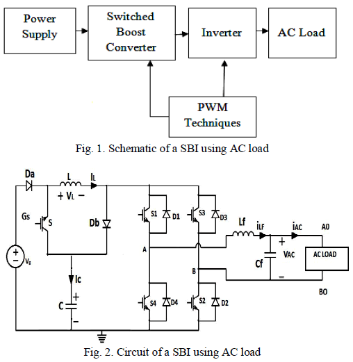
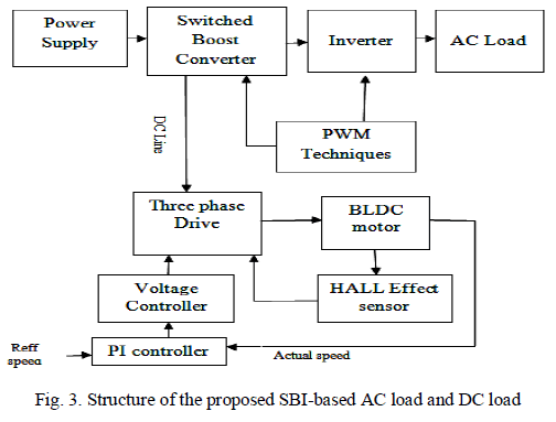
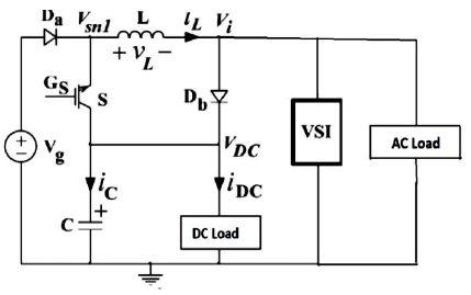
| The schematic of the SBI in which a switched boost
network comprising of one active switch (s),two diodes
(Da.Db), one inductor (L), and capacitor(C) is connected
between voltage source Vg and the inverter bridge. A
low-pass LC filter is used at the output of the inverter
bridge to filter the switching frequency components in the
inverter output voltage. |
SWITCHED BOOST INVERTER TOPOLOGY FOR
AC AND DC LOADS |
 |
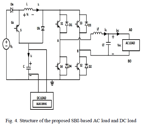 |
| Three different power converter stages are used to
interface the renewable energy source, energy storage unit,
and the local AC loads in the system to the DC bus. This
paper proposes a structure of the variable speed operation
using switched boost inverter (SBI) as a power electronic,
interface. The structure of the proposed SBI-based variable
speed BLDC motor [4] shows the circuit diagram of the
SBI supplying both DC and AC loads. |
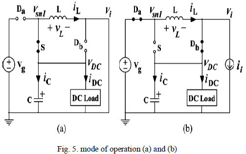 |
| mode I To explain the steady-state operation of the
SBI, assume that the inverter is in a shoot-through zero
state for duration D. TS in a switching cycle TS. The
switch S is also turned on during this interval. As shown
in the equivalent circuit of Fig.5(a) the inverter bridge is
represented by a short circuit during this interval. The
diodes DA and Deb are reverse biased (as VC > VG), and
the capacitor C charges the inductor L through switch S
and the inverter bridge. The inductor current in this
interval equals the capacitor discharging current. |
| mode II For the remaining duration of the switching
cycle (1 −D). TS, the inverter is in non-shoot-through
state, and the switch S is turned off. The inverter bridge is
represented by a current source in this interval as shown
in the equivalent circuit of Fig. 5 (b) now, the voltage
source VG and inductor L together supply power to the
inverter and the capacitor through diodes DA and DB.
The inductor current in this interval equals the capacitor
charging current added to the inverter input current. Note
that the inductor current is assumed to be sufficient
enough for the continuous conduction of diodes DA and
DB for the entire interval (1 − D). TS. |
 |
| Fig.6. Connection of a VSI across the switching terminal Vi of the
CIWJ topology (switch Si can be realized by using the shoot-through
state of the VSI). |
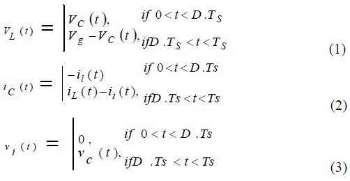 |
| Using small ripple approximation, (1) –(3) can be
rewritten as Note that similar to a ZSI the shoot-through
duty ratio(D) of the SBI also cannot exceed 0.5 for a
positive DC bus voltage, VDC. |
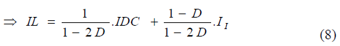
| Here, VDC, IL , and IDC are DC components in VDC
(t), IL (t), and IDC (t), respectively, and I am the current
drawn by inverter bridge in (1 − D) ·TS interval |
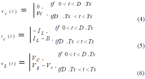 |
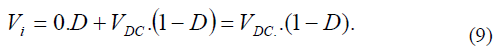
| Under steady state, the average voltage across the
inductor and average current through the capacitor in one
switching cycle should be zero. Using volt second
balance, we have |
 |
| Similarly, using charge-second balance, one can write |
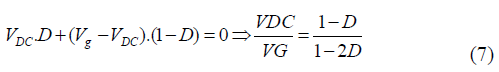
 |
| The average DC link voltage VI can be calculated as |
 |
| A. SBI has following advantages: |
| 1)In the event of shoot-through in any phase leg of the
inverter bridge, the diode Db is reverse-biased and
capacitor C is disconnected from the inverter bridge.
Now, the current through the circuit is limited by the
inductor L. So, similar to ZSI, shoot-through does
not damage the switches of the SBI. |
| 2)As the SBI allows shoot-through, no dead-time is
needed to protect the converter. Also this circuit
exhibits better EMI noise immunity compared to a
VSI. |
| 3) Since dead-time is not required, there is no need of
extra dead-time compensation technologies to
compensate the waveform distortion caused by
dead- time. |
PWM CONTROL OF SBI |
| The SBI utilizes the shoot-through interval of the Hbridge
to invoke the boost operation. So, the traditional
PWM techniques of VSI [9],[12] [14] have to be modified
to incorporate the shoot-through state, so that they are
suitable for SBI. In [6],a PWM scheme for SBI is
developed based on the traditional sine-triangle PWM with
uni polar voltage switching [9],[12],[14]. |
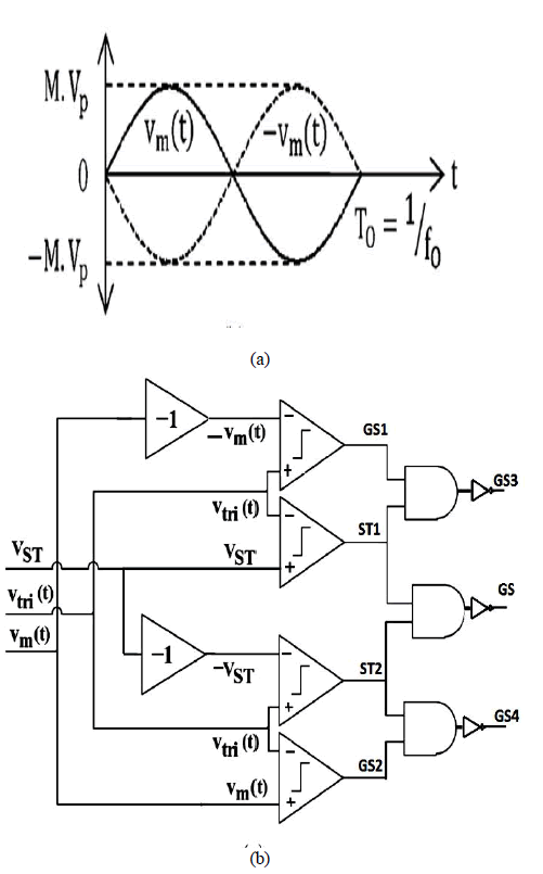
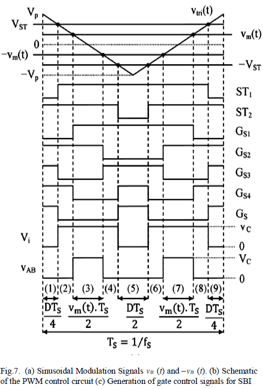
| This technique has been illustrated in Fig. 7 during positive
and negative half cycles of the sinusoidal modulation signal
vm(t) |
| As shown in Fig. 7(b) and (c), the gate control signals
GS 1 and GS 2 are generated by comparing the sinusoidal
modulation signals vm(t), and –vm(t) shown in Fig. 7(a)
with a high-frequency triangular carrier vtri(t) of amplitude
Vp . The frequency fS of the carrier signal is chosen such
that fS >fO. |
| Therefore, vm(t)is assumed to be nearly constant in Fig.
7(c). The signals ST1and ST2 are generated by comparing
vtri(t) with two constant voltages VST and –VST,
respectively. The purpose of these two signals is to insert
the required shoot-through interval D·TS in the PWM
signals of the inverter bridge. Now the gate control signals
for switches S3 , S4 , and S can be obtained using the
logical expressions given as follows: |
| GS3 =GS2+ST1; GS4 =GS1 +ST2; GS = ST1 +ST2 . (10) |
| Similarly, as shown in Fig. 7 (c), the gate control signals
GS3 and GS4 are generated by comparing the modulation signals –vm(t), and vm(t) with the triangular carrier vtri(t).
The shoot-through signals ST1 and ST2 are generated in
the same manner as in the positive half cycle. The gate
control signals for switches S1 , S2 , and S can be obtained
using the logical expressions given as follows: |
| GS1 =GS4+ST1 ; GS2 =GS3 +ST2 ; GS = ST1 +ST2 (11) |
| It can be observed from Fig. 7 that, during positive
half cycle of vm(t), the shoot-through signals ST1, ST2 are
logically added toGS2 , GS1 , respectively, while in
negative half cycle of vm(t), these signals are logically
added toGS4,GS3, respectively take care that all four
switches of the inverter bridge equally participate in
generating the shoot-through interval. Note that with this
PWM control technique, the shoot-through state of the
inverter bridge will have no effect on the harmonic
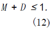
spectrum of the inverter’s output voltage Vab, if the sum of
shoot-through duty ratio (D) and the modulation index (M)
is less than or equal to unity [6], i.e., |
 |
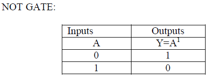
| Here logical operation of the OR gates and NOT gate
operation for PWM Techniques. |
 |
 |
 |
 |
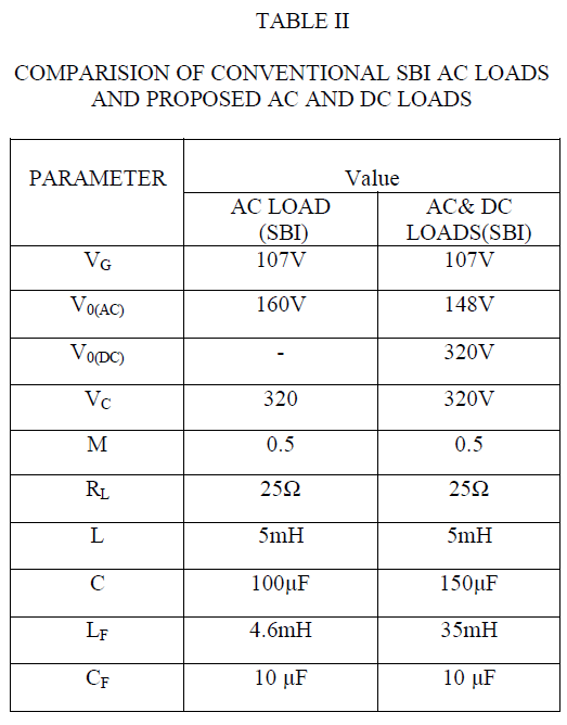
COMPARISION OF CONVENTIONAL SBI AC
LOADS AND PROPOSED AC AND DC LOADS |
| This section presents the comparison of conventional
system .the input voltage, capacitor voltage, output voltage.
here Table II shown the parameters used for the
comparison of both AC and DC loads. All parameter
verified using MATLAB simulation of the SBI circuits. |
| A. Comparison of Shoot-Through Tolerance Due to
EMI Noise |
| In a ZSI, if there is a shoot-through in the inverter
bridge either by fault or due to EMI noise,[2],[3]. the
shoot-through current is limited by the impedance network,
and the inverter switches will not be damaged, which is not
the case with a traditional H-bridge VSI. Similarly, in SBI
also, if there is a shoot-through in the inverter bridge either by fault or due to EMI noise, the shoot through current is
limited by the inductor L, and the inverter switches will not
be damaged. Therefore, similar to ZSI, the SBI also has
shoot-through tolerance and thus exhibits better EMI noise
immunity compared to the traditional VSI. |
| B. Comparison of SBI with a Traditional Two-Stage DC-to-
AC Conversion System |
| In the previous section, it is shown that the SBI is a single
input, two-output (one dc output and one ac output) power
converter derived from IWJ converter and a VSI. Similar to
the traditional two- stage dc to dc conversion system [7].
The SBI can also generate an ac output voltage that is
either the greater or less than the input dc voltage.
However, the SBI has the advantages and limitations when
compared to the two stage DC to DC, DC to AC
conversion system |
 |
| 1) Dead-Time Requirement: A shoot-through event in the
inverter bridge of the two-stage conversion system
damages the power converter stage, as well as the dc loads connected to the dc bus . So a dead-time circuit is
necessary t0Ominimize the occurrence of shoot-through
events in this system. Moreover, to compensate the
waveform distortion caused by dead-time, one has to
use the complex dead-time compensation technologies
[13]. This is not the case with SBI, as it allows shootthrough
in the inverter phase legs. So the use of SBI
eliminates the need for a dead-time circuit as well as the
requirement of dead-time compensation technologies. |
| 2) Reliability and EMI Noise Immunity: Even with a dead
time circuit, the probability of a shoot-through event
cannot be eliminated completely because an EMI noise
can also cause shoot-through in the inverter phase legs
[2],[3],[11].With the use of SBI, the shoot-through
event does not damage the switches of the power
converter. So, SBI exhibits better EMI noise immunity
and hence has better reliability compared to the twostage
conversion system. |
| 3) Extreme Duty Cycle Operation: At the extreme duty
ratio operation (e.g., for D ≥ 0.75) of a conventional
boost converter, the inductor L is charged over a longer
time duration in the switching cycle, and very small
time interval is left to discharge the inductor through the
output diode Db . So this diode should sustain a short
pulse width current with relatively high amplitude.
Also, this causes severe diode reverse recovery current
and increases the EMI noise levels in the converter
[11]–[14],This also imposes a limit on the switching
frequency of the boost converter and thus increases the
size of the passive components used in the two-stage
conversion system. so, even when the converter
operates at the point of maximum conversion ratio, the
conduction time of the diodes Da , Db of SBI is
approximately equal to 50% of the switching time
period, which alleviates the problems due to extreme
duty ratio 0peration of a boost converter. So, SBI can
operate at relatively higher switching frequencies
compared to the traditional two stage conversion
system. |
| 4) Number of Control Variables: Similar to a two-stage
conversion system, the SBI also has two control
variables: Shoot through duty ratio (D) and the
modulation index (M).The dc bus voltage VDC is
controlled by D, while ac output voltage of the
converter is controlled by M. However, similar to ZSI
[7], the value one of these two control variables decides the upper limit of the second control variable of SBI.
The mathematical relation between D and M depends
on the control technique used. Note that, as mentioned
above, it is possible to extend most of the PWM control
techniques of ZSI [12]–[14] to control the SBI also. |
| 5) Number of Devices: As shown in Fig. 3, the SBI requires
five active switches, six diodes, two inductors, and two
capacitor for its realization. The two-stage conversion
system shown in Fig. 6 uses only one diode (Da ) less
compared to the SBI. However, in a dc application, the
input comes from a renewable energy source, e.g., solar
panel or fuel cell, which should always be associated
with a series diode to block the reverse power flow [2],
[3]. So the diode Da of SBI can be a part of the
renewable energy source which eliminates the need for
an external diode. Thus, the number of devices in both
converters is same. |
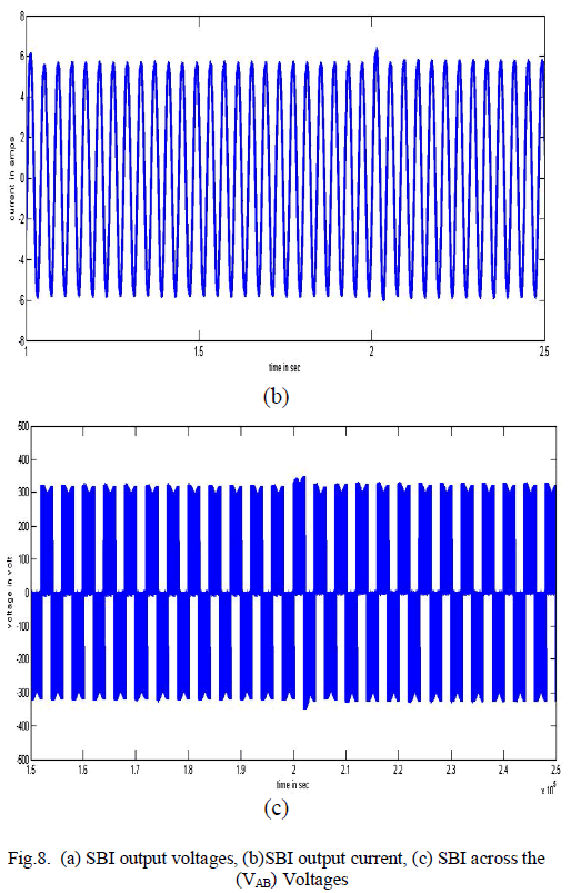
SIMULATION VERIFICATION |
| Here discussed shows the Fig. 3 architecture of the SBI
supplying both dc and ac loads. In this scheme, the task of
the PWM controller is to generate gate control signals
pulse(GS , GS 1 , GS 2 ,GS 3 , and GS 4 ) for SBI ,such that the
voltages at the dc bus (VDC) and the ac bus (vAC), |
| A. AC output for (R LOAD) |
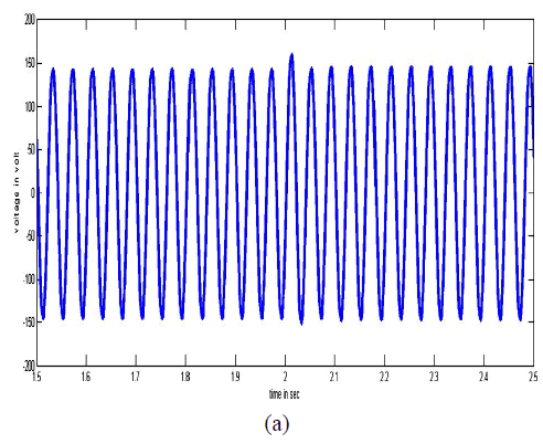 |
 |
| B. DC output voltages for( BLDC motor drive) |
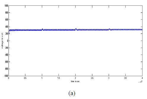 |
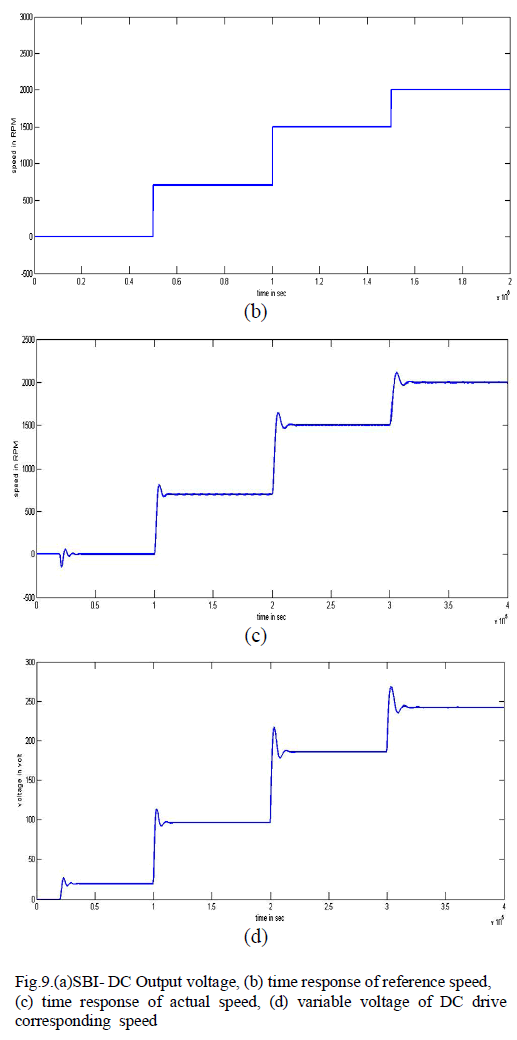 |
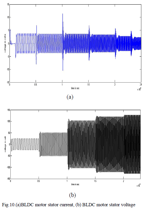 |
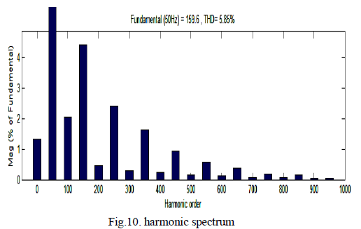
| C. Harmonic spectrum of output voltage |
| The harmonic spectrum of the output voltages showed
Fig.10. The harmonic spectrum of the inverter’s output
voltages (VAB) with D=0.4; M= 0.5 the method of
comparing the effectiveness of modulation is by comparing
the unwanted components i.e., The distortion in the output
voltage or current waveform, the relative to that of an ideal
sine wave, it can be assumed that with proper control, the
positive and negative portions of the output are
symmetrical (no DC or harmonics). |
 |
CONCLUSION |
| The work has presented a novel power electronic
interface called Switched Boost Inverter (SBI) for motor
drive applications. It is shown that the SBI is a single-stage
power converter that can supply both DC and AC loads
simultaneously from a single DC input. Describes the
advantages and limitations of SBI when compared to the
ZSI and the traditional two - stage DC to AC conversion
system. The steady-state and small-signal analysis of the
SBI supplying both DC and AC loads, and a PWM control
technique suitable for SBI are also described. The
performance of SBI has been tested experimentally with an
isolation transformer and also with three different types of
AC loads: R, RL, and nonlinear loads. It can be concluded
from the experimental results that the control strategy of
SBI shows excellent performance during steady state as
well as during a step change in either DC or AC load in the
system. These results confirm the suitability of SBI and its
open-loop control strategy for motor drive applications. |
References |
- R. Adda, S. Mishra, and A. Joshi, âÃâ¬ÃÅA PWM control strategy forswitched boost inverter,âÃâ¬Ã in Proc. 3rd IEEE Energy Convers. Congr.Expo.,Phoenix,AZ, 2011, pp. 4208âÃâ¬Ãâ4211.
- F. Z. Peng, âÃâ¬ÃÅZ-source inverter,âÃâ¬Ã IEEE Trans. Ind. Appl., vol. 39, no.2,pp. 504âÃâ¬Ãâ510, Mar./Apr. 2003.
- Y. Huang, M. Shen, F. Z. Peng, and J. Wang, âÃâ¬ÃÅZ-source inverter forresidentialVphotovoltaic systems,âÃâ¬Ã IEEE Trans. Power Electron.,vol. 21, no. 6,Vpp. 1776âÃâ¬Ãâ1782, Nov. 2006.
- F. Z. Peng, âÃâ¬ÃÅZ-source inverter for adjustable speed drives,âÃâ¬Ã IEEEPower Electron. Lett., vol. 1, no. 2, pp. 33âÃâ¬Ãâ35, Jun. 2003.
- Z. J. Zhou, X. Zhang, P. Xu, andW. X. Shen, âÃâ¬ÃÅSingle-phaseuninterruptibleVpower supply based on Z-source inverter,âÃâ¬Ã IEEETrans. Ind. Electron.,Vvol. 55, no. 8, pp. 2997âÃâ¬Ãâ3004, Aug. 2008.
- S. Upadhyay, S. Mishra, and A. Joshi, âÃâ¬ÃÅA wide bandwidth electronicload,âÃâ¬Ã IEEE Trans. Ind. Electron., vol. 59, no. 2, pp. 733âÃâ¬Ãâ739, Feb.2012.
- J. Liu, J. Hu, and L. Xu, âÃâ¬ÃÅDynamic modeling and analysis of Zsource converter-derivation of ac small-signal model and designorientedanalysis,âÃâ¬Ã IEEE Trans. Power Electron., vol. 22, no. 5, pp.1786âÃâ¬Ãâ1796, Sep. 2007.
- R. W. Erickson and D. Maksimovic, Fundamentals of PowerElectronics, 2nd ed. Norwell, MA: Kluwer, Jan. 2001.
- N. Mohan, T. Undeland, and W. Robbins, Power Electronics:Converters, Applications and Design, 2nd ed. New York: Wiley,1995.
- P. C. Loh, D. Vilathgamuva, Y. S. Lai, G. Chua, and Y. Li, âÃâ¬ÃÅPulsewidthmodulation of Z-source inverters,âÃâ¬Ã IEEE Trans. PowerElectron., vol. 20, no. 6, pp. 1346âÃâ¬Ãâ1355, Nov. 2005.
- S. Mishra, R. Adda, and A. Joshi, âÃâ¬ÃÅInverse Watkins-Johnsontopology based inverter,âÃâ¬Ã IEEE Trans. Power Electron., vol. 27, no.3, pp. 1066âÃâ¬Ãâ 1070, Mar. 2012
- D. G. Holmes and T. A. Lipo, Pulse Width Modulation for PowerConverters: Principles and Practice. Piscataway, NJ: IEEE Press,2003.
- S. H. Hwang and J. M. Kim, âÃâ¬ÃÅDead-time compensation methodvoltage fed PWM inverter,âÃâ¬Ã IEEE Trans. Energy Convers., vol. 25, no. 1, pp. 1âÃâ¬Ãâ10,Mar. 2010002E
- P. C. Loh, D. Vilathgamuva, Y. S. Lai, G. Chua, and Y. Li, âÃâ¬ÃÅPulsewidthmodulation of Z-source inverters,âÃâ¬Ã IEEE Trans. PowerElectron., vol. 20, no. 6, pp. 1346âÃâ¬Ãâ1355, Nov. 2005.
|