International Journal of Innovative Research in Science, Engineering and Technology
ISSN ONLINE(2319-8753)PRINT(2347-6710)
ISSN ONLINE(2319-8753)PRINT(2347-6710)
| V. Parthibaraj, K. Tamilarasan, K. S. Pugazhvadivu, C. Rangasami Department of Physics, Kongu Engineering College, Perundurai, Erode, Tamil Nadu, India |
| Related article at Pubmed, Scholar Google |
Visit for more related articles at International Journal of Innovative Research in Science, Engineering and Technology
Polycrystalline Cu2ZnSnS4 (CZTS) thin film has been grown on glass substrate by RF-magnetron sputtering at substrate temperature 573 K using a commercial target of same composition. Structural and optical properties of the grown thin film have been investigated by X-ray diffraction (XRD), scanning electron microscope (SEM), Raman spectroscopy and UV-vis spectroscopy. Detailed analysis of XRD data has showed that the as-grown CZTS thin film has keserite structure ( I 4 , a = 5.4290 and c = 10.849Å) with preferred orientation along (112) plane. All the peaks observed in the XRD pattern have been accounted for kieserite structure, which shows the absence of additional phases such as elemental or binary or ternary systems in the grown film. SEM images recorded with different magnification have showed that the film has smooth and homogeneous surface with average crystallite size 100 nm. Raman spectrum recorded at room temperature has showed the dominant Raman shift at about 326 cm-1 which can be attributed to A1 mode and confirms the formation of kieserite CZTS phase. From optical transmittance spectrum, the grown film is found to have direct band gap of ~1.51 eV. The above observations show that the material under investigation is suitable for solar cell application.
Keywords |
| Cu2ZnSnS4; RF magnetron sputtering; XRD; SEM; Raman spectroscopy and Optical band gap. |
INTRODUCTION |
| Cu2ZnSnS4 has emerged as one of the promising absorber layer materials for thin film solar cell application, because it exhibits a near-optimum direct band gap of ~ 1.5 eV and has a large absorption coefficient in the order of 104 cm-1 [1]. Moreover, the constituent elements of CZTS are earth-abundant and non-toxic in nature. On the other hand, CuInGaSe2 (CIGS) has also been studied extensively for more than a decade towards solar application as it exhibit a band gap in the range 1.0 eV (CuInSe2) to ~ 1.7 eV (CuGaSe2) [2]. Recently, the highest conversion efficiency (CE) of 20.4 % has been reported for CIGS absorber based thin film solar cells [3]. However, the constituent elements of CIGS are very expensive and some of them are highly toxic in nature. This leads to high commercialisation cost and hence, hamper the large scale usage in industries and agriculture, and also for home appliances. At present, CZTS has been given much attention towards solar cell application and in fact, it is recognized an excellent alternate for CIGS based on the above said factors. Therefore, Cu2ZnSnS4 can be considered as an exceptional material for thin film solar cell application. |
| As yet, Todorov et al have reported [4] the CE of 9.6 % for CZTS based thin film solar cell. They have grown the thin films by simple ink based technique. Again, in 2012, they have developed CZTS based solar cell capable of converting 11.1% of solar energy into electricity [5]. Recently, they have developed a CZTS solar cell which exhibits a CE of 12.6 % jointly with the Japanese thin-film solar company - Solar Frontier, IBM and Tokyo Ohka Kogyo [6]. It is worth to mention here that active researches towards the enhancement of CE of CZTS based solar cells are undertaken by several organizations at present. |
| CZTS can be derived by replacing the first half of In atom with Zn atom and the other half with Sn atom in the chalcopyrite lattice of CuInS2. Compared to the conversion efficiencies reported for CIGS absorber layer based single junction thin film solar cells, the efficiencies achieved with CZTS based solar cells are much less. To overcome this, a systematic research on optimization of growth parameters, materials properties and the structure of solar cell is inevitable to achieve required stoichiometry of constituent elements. In fact, CZTS based thin film solar cells have not been studied extensively for several years due to the lack of understanding of the growth parameters governing the cell performance. Moreover, the concept of nanotechnology is not intensively imparted towards the enhancement of conversion efficiency. Up to now, CZTS thin films are generally prepared by thermally activated processes like evaporation and sequential processing which is comprised of deposition of the alloy precursors followed by postannealing. The former method includes both multi-stage [7] and co-evaporation of precursor [8, 9], which are very difficult to scale up. In the latter technique, the precursors can be deposited by various methods such as atom beam sputtering [10], electron beam evaporation [11, 12], RF sputtering [13, 14], hybrid sputtering [15], pulsed laser deposition [16], photo- chemical deposition [17], sol–gel [18], spray pyrolysis [19-21], electro deposition [22, 23] and soft-chemistry [24]. Among these methods, sputtering technique yields thin films with (i) high uniformity, (ii) ideal stoichiometric ratio of constituent elements, (iii) pre-determined film thickness, (iv) smaller grain size with different orientations, (v) better adhesion, (vi) high deposition rate, (vii) higher surface mobility in condensing particles, and (ix) high smooth and conformal film morphologies. Now-a-days, most of the researchers choose RF magnetron sputtering method for growing CZTS thin films solar cell application. But no reports especially on the optimization of growth parameters of CZTS thin film for high efficiency solar cells are available in the literature. As a part of the optimization process, crystal structure, microstructure and optical properties of CZTS thin film grown by RF magnetron sputtering have been investigated using XRD, SEM and UV vis spectroscopy in the present work. |
EXPERIMENTAL |
| CZTS thin films were deposited on glass substrate by RF magnetron sputtering using commercially available (purchased from Opetech Chemicals Co.Ltd., Hsinchu, Taiwan) sputtering target which is composed of finely mixed Cu2S, ZnS and SnS2 with ratio 2:1.5:0.5. The growth parameters such as sputtering power, working pressure, target and substrate distance and sputtering time were fixed at 75Watt, 10-5 mTorr, 3 cm and 30 minutes, respectively. The film was grown in argon ambient with partial pressure of 10-3 mTorr. The crystal structure and crystallite size of the grown thin film were determined using XRD data obtained from X-ray diffractometer (XPert with CuKα radiation) and Debye Scherer formula, respectively. The surface morphology and compositional ratio of the film material were observed by SEM (Hitachi S-4100, provided with EDAX). The optical transmittance spectrum of the thin film was recorded with an UV-vis Spectrophotometer (UV-VIS-JASCO) in the wavelength range of 400–2500 nm. |
RESULTS AND DISCUSSION |
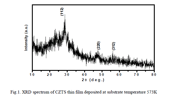
| The XRD pattern of CZTS thin film grown at substrate temperature 573 K is shown in fig. 1. Presence of multiple peaks in the XRD pattern confirms the polycrystalline nature of grown thin film. The peaks observed at 2θ values around 28, 47 and 56° respectively correspond to (112), (220) and (312) diffraction planes of CZTS. The reflections from these planes are recognized as characteristics of Cu2ZnSnS4 with tetragonal kesterite structure (JCPDS card no. 26-0575). The XRD pattern does not contain peaks corresponding to any secondary phases or constituent elements, which confirms that the prepared film is homogenous and single phase. The dominant peak observed at 2θ = 28.694° is due to the reflection from a plane with preferred orientation (112). The lattice parameters were calculated to be a = 5.4290 A ° and c = 10.849 A ° using plane-spacing equation and are in good agreement with the reported lattice parameters a = 5.427 A ° and c = 10.848 A ° (JCPDS, card no. 26-0575). |
 |
| The crystallite size of the film was calculated using the Debye Scherer’s equation. |
| D= K λ / β cosθ (1) |
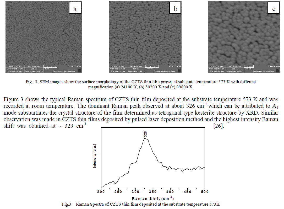
| where λ, β and θ are respectively the wave length of X-ray radiation, FWHM of a selected peak and the corresponding Bragg’s diffraction angle. The average crystallite size of Cu2ZnSnS4 the thin film was estimated to be 100 nm. These observations suggest that the grown CZTS film has elemental concentration close to stoichiometric ratio. Being as a quaternary compound CZTS, it is difficult to control the compositional ratio close to stoichiometry. Thus it requires additional control over synthesis parameters to obtain the desired phase of the material. However, the film with elemental composition close to expected stoichiometric ratio was achieved with RF magnetron sputtering in the present work. Thus, a detailed analysis of XRD data has showed that the as-grown Cu2ZnSnS4 thin film has crystallized in keserite structure ( I 4 ) with preferred orientation along (112) plane. The film thickness was determined to be of about 400 nm by gravimetric method. The surface morphology of CZTS film deposited at the substrate temperature 573 K was analysed by recording SEM images with different magnification. The SEM images are shown in fig. 3. Figure 3a is the SEM image recorded with magnification 24100 X whereas the SEM images shown in fig. 3b and 3c respectively recorded with magnification 50200 X and 89800 X. Figure 3c shows clearly the presence of spherical shaped nanoparticles with uniform distribution and small voids rarely. In conclusion, the SEM images reveal that the grown film has homogeneous, highly polycrystalline and extremely dense morphology without any bigger voids. Similar kind of observation was made with a polycrystalline film of thickness 800 nm grown on soda-lime glass substrates by a reactive magnetron co-sputtering technique [25]. |
 |
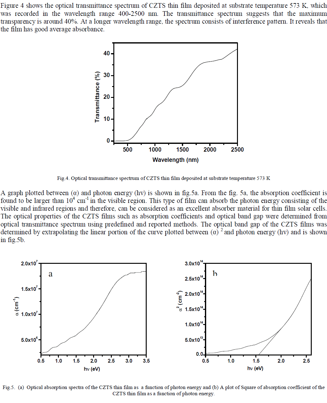 |
| The estimated direct optical band gap of the CZTS films is about 1.51 eV. This band gap value is quiet close to the optimal band gap required for a solar cell absorber layer. The value of band gap is in good agreement with the band gaps reported for CZTS films [27-32]. |
CONCLUSION |
| CZTS thin film has been successfully grown on glass substrate by RF magnetron sputtering and is characterized by XRD, Raman spectroscopy, SEM, and optical transmittance measurements. The X-ray diffraction pattern of CZTS (stoichiometry close to Cu2ZnSnS4) thin film has revealed that the film has crystallized in tetragonal type kesterite structure with space group ( I 4 ). The peaks present in the XRD pattern indicate that the film has good crystalline nature and has strong preferred oriented along (112) plane. The SEM analysis shows that the film has homogeneous and dense surface morphology, and consists of large number of crystallites throughout the film. The dominant Raman peak observed at about 329 cm-1 substantiates the XRD results well. Analysis of UV–visible spectroscopy data has revealed that the CZTS film has an absorption coefficient in the order of about 104 cm−1. The direct optical band-gap energy of the CZTS thin film is determined to be ~1.51 eV, which is very close to the optimum value for a good solar-cell absorber. The structural and optical properties have showed that the CZTS thin film is suitable for solar cell applications. |
References |
|