International Journal of Innovative Research in Science, Engineering and Technology
ISSN ONLINE(2319-8753)PRINT(2347-6710)
ISSN ONLINE(2319-8753)PRINT(2347-6710)
T. Rupalatha1, Mr.C.Leelamohan2, Mrs.M.Sreelakshmi3
|
| Related article at Pubmed, Scholar Google |
Visit for more related articles at International Journal of Innovative Research in Science, Engineering and Technology
Edge detection is one of the basic operation carried out in image processing and object identification.In this paper, we present a distributed Canny edge detection algorithm that results in significantly reduced memory requirements, decreased latency and increased throughput with no loss in edge detection performance as compared to the original Canny algorithm. The new algorithm uses a low-complexity 8-bin non-uniform gradient magnitude histogram to compute block-based hysteresis thresholds that are used by the Canny edge detector. Furthermore, an FPGA-based hardware architecture of our proposed algorithm is presented in this paper and the architecture is synthesized on the Xilinx Spartan-3E FPGA. Simulation results are presented to illustrate the performance of the proposed distributed Canny edge detector. The FPGA simulation results show that we can process a 512×512 image in 0.287ms at a clock rate of 100 MHz.
Keywords |
| Canny Edge detector, Distributed Processing, Non-uniform quantization, FPGA. |
INTRODUCTION |
| Edge detector in [1] offers a trade-off between precision, cost and speed, and its capability to detect edges is not as good as the Canny algorithm. There is another set of work on Deriche filters that have been derived using Canny’s criteria. For instance, it was stated in [2] that a network with four transputers takes 6s to detect edges in a 256×256 image using the Canny- Deriche algorithm, far from the requirement for real-time applications .The approach of [3] operates on two rows of pixels at a time. This reduces the memory requirement at the expense of a decrease in the throughput. Furthermore, it is known that the original Canny edge detection algorithm needs two adaptive imagedependent high and low thresholds to remove false edges. However, the algorithm in [3] just fixes high and low thresholds in order to overcome the dependency between the blocks, which results in a decreased edge detection performance. In [4], we proposed a new threshold selection algorithm based on the distribution of pixel gradients in a block of pixels to overcome the dependency between the blocks. However, in [4], the hysteresis thresholds calculation is based on a very finely and uniformly quantized 64-bin gradient magnitude histogram, which is computationally expensive and, thereby, hinders the real-time implementation. In this paper, a method based on non-uniform and coarse quantization of the gradient magnitude histogram is proposed. |
II. CANNY EDGE DETECTION ALGORITHM |
| Canny developed an approach to derive an optimal edge detector based on three criteria related to the detection performance. |
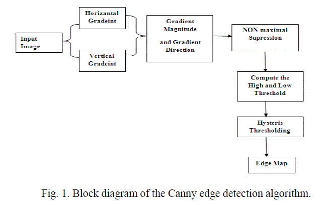 |
| A block diagram of the Canny edge detection algorithm is shown in Fig. 1. The original Canny algorithm [5] consists of the following steps: 1. Smoothing the input image by Gaussian mask. The output smoothed image is denoted as I(x, y). 2. Calculating the horizontal gradient Gx(x, y) and vertical gradient Gy(x, y) at each pixel location by convolving the image I(x, y) with partial derivatives of a 2D Gaussian function. 3. Computing the gradient magnitude G(x, y) and direction θG(x, y) at each pixel location. 4. Applying non-maximum suppression (NMS) to thin edges. 5. Computing the hysteresis high and low thresholds based on the histogram of the magnitudes of the gradients of the entire image. 6. Performing hysteresis thresholding to determine the edge map. |
III. PROPOSED DISTRIBUTED CANNY EDGE DETECTION ALGORITHM |
| The Canny edge detection algorithm operates on the whole image and has a latency that is proportional to the size of the image. In [4], we proposed a distributed Canny edge detection algorithm, which removes the inherent dependency between the various blocks.Steps 1,4,6 of the distributed Canny algorithm are the same as in the original Canny that are now applied at the block level. Step 5, which is the hysteresis high and low thresholds calculation, is modified to enable parallel processing. In [4], a parallel hysteresis thresholding algorithm was proposed based on the observation that a pixel with a gradient magnitude of 2, 4 and 6 corresponds to blurred edges. |
 |
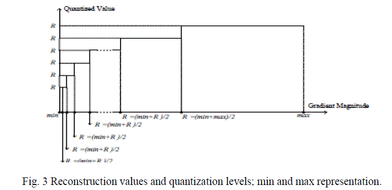 |
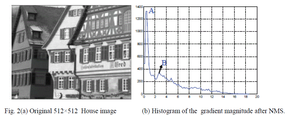
| A sample gradient magnitude histogram is shown in Fig. 2(b) for the 512×512 House image (Fig. 2(a)). Based on the above observation, we propose a non-uniform quantizer to discretize the gradient magnitude histogram. Specifically, the quantizer needs to have more quantization levels in the region between the largest peak A and B and few quantization levels in other parts. Fig. 3 shows reconstruction levels can be computed. |
IV. PROPOSED DISTRIBUTED CANNY ALGORITHM IMPLEMENTATION ON FPGA |
| In this section, we describe the hardware implementation of our proposed distributed Canny edge detection algorithm on the Xilinx Spartan-3E FPGA. A. Architecture Overview |
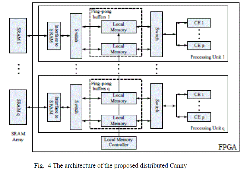 |
| Depending on the available FPGA resources, the image needs to be partitioned into q sub-images and each sub-image is further divided into p m x m blocks. The proposed architecture, shown in Fig.4, consists of q processing units in the FPGA and some Static RAMs (SRAM) organized into q memory banks to store the image data.Thus, p × q blocks can be processed at the same time and the processing time for an N×N image is reduced, in the best case, by a factor of p x q. |
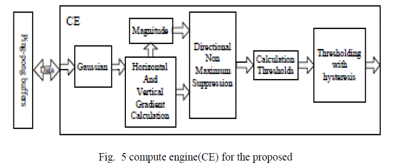 |
| The specific values of p and q depend on the processing time of each PE, the data loading time from the SRAM to the local memory and the interface between FPGA and SRAM, such as total pins on the FPGA, the data bus width, the address bus width and the maximum system clock of the SRAM. B. Image Smoothening The input image is smoothened using a 3×3 Gaussian mask, as shown in Fig. 6(a). The Gaussian filter (Fig. 6a) is separable and, thus, the implementation of the 2-D convolution with the 3×3 Gaussian mask is achieved using row and column 1- D convolutions. The proposed architecture for the smoothening unit is shown in Fig. 6(b). |
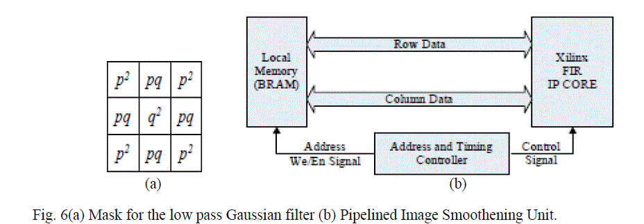 |
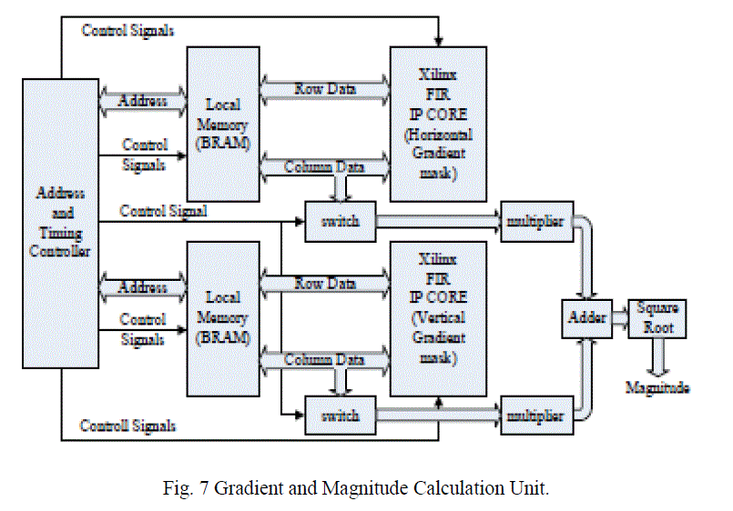
| Fig. 6(a) Mask for the low pass Gaussian filter (b) Pipelined Image Smoothening Unit. The main components of the architecture consists of a 1-D finite impulse filter (FIR) to process the data and the on-chip Block RAM (BRAM) to store the data. In our design, we adopt the Xilinx’s pipelined FIR IP core, which provides a highly parameterizable, area-efficient, high-performance FIR filter utilizing the structure characteristics in the coefficient set, such as symmetry and conjugacy . C. Gradients and Gradient Magnitude Calculation This stage calculates the vertical and horizontal gradients using convolution kernels. The kernels vary in size from 3×3 to 9×9, depending on the sharpness of the image. The Xilinx FIR core, which can support up to 256 sets of coefficients with 2 to 1024 coefficients per set, is used to implement the kernels. The architecture of this unit is shown in Fig7. The gradient calculation architecture consists of two 1-D FIR models and the corresponding local memory. The filters for computing the horizontal and vertical gradient elements can process data in parallel. |
 |
| D. Directional Non Maximum Suppression Fig. 8 shows the architecture of the directional NMS unit. In order to access all the pixels’ gradient magnitudes in the 3×3 window at the same time, two FIFO buffers are employed. |
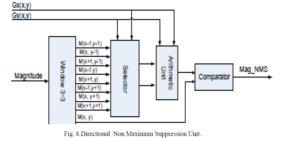 |
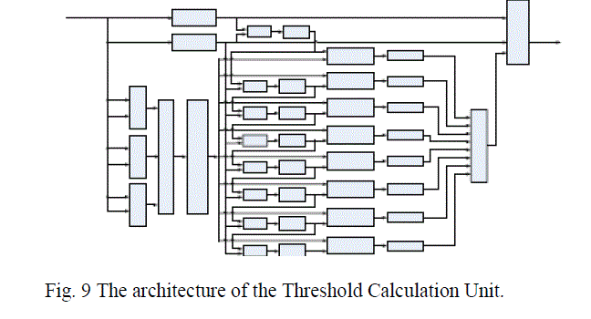
| The horizontal gradient Gx and the vertical gradient Gy control the selector which delivers the gradient magnitude (marked as M(x, y) in Fig. 8) of neighbours along the direction of the gradient, into the arithmetic unit. E. Calculation of the hysteresis thresholds: Since the low and high thresholds are calculated based on the gradient histogram, we need to compute the histogram of the image after it has undergone directional non-maximum suppression .As discussed in Section 3, an 8- step non-uniform quantizer is employed to obtain the discrete histogram for each processed block. |
 |
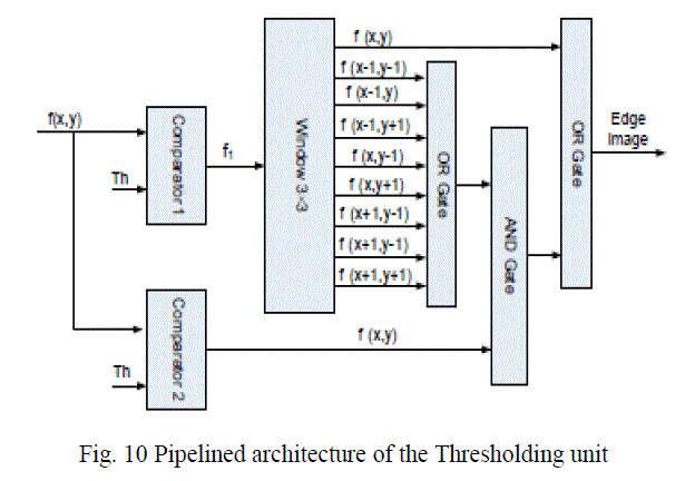
| F. Thresholding with hysteresis Since the output of the non maximum suppression unit contains some spurious edges, the method of thresholding with hysteresis is used. Two thresholds, high threshold ThH and low threshold ThL , which are obtained from the threshold calculation unit, are employed. Let f(x, y) be the image obtained from the non maximum suppression stage, f1(x, y) be the strong edge image and f2(x, y) be the weak edge image. |
 |
V. SIMULATION RESULTS |
| The algorithm performance was tested using a variety of512×512 natural images. A. Mat lab Simulation Results ( |
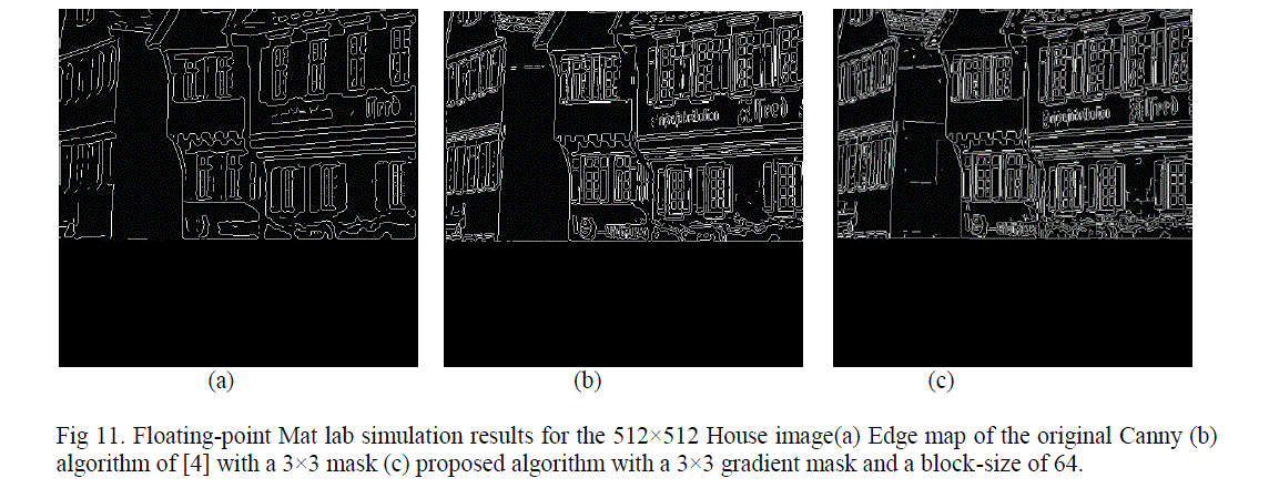 |
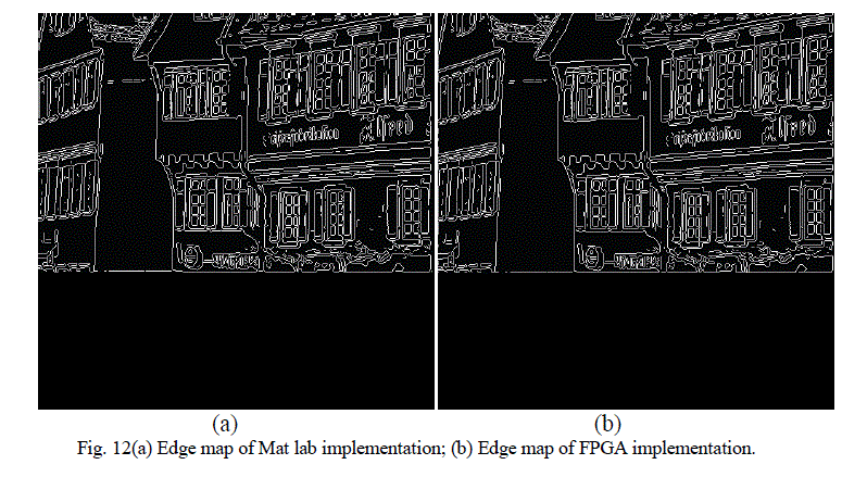
| Fig 11. Floating-point Mat lab simulation results for the 512×512 House image(a) Edge map of the original Canny (b) algorithm of [4] with a 3×3 mask (c) proposed algorithm with a 3×3 gradient mask and a block-size of 64. B. Fixed-point Mat lab and FPGA Simulation Results Fig.12 shows the fixed-point Mat lab implementation software result and the FPGA implementation generated result for the 512×512 House image using the proposed distributed Canny with block size of 64×64 and a 3×3gradient mask. The FPGA result is obtained using Model Sim . Furthermore, for a 100MHz clock rate, the total processing running time using the FPGA implementation is 0.287ms for a 512×512 image. |
 |
VI. CONCLUSION |
| We presented a novel distributed Canny edge detection algorithm that results in a significant speed up without sacrificing the edge detection performance.As a result, the computational cost of the proposed algorithm is very low compared to the original Canny edge detection algorithm. The algorithm is mapped to onto a Xilinx Spartan-3E FPGA platform and tested using Model Sim. |
References |
|