International Journal of Innovative Research in Science, Engineering and Technology
ISSN ONLINE(2319-8753)PRINT(2347-6710)
ISSN ONLINE(2319-8753)PRINT(2347-6710)
N.Lavanya1, S.Sindhu Meenakshi2
|
| Related article at Pubmed, Scholar Google |
Visit for more related articles at International Journal of Innovative Research in Science, Engineering and Technology
A fast-locking pulsewidth-controlled clock generator (PWCCG) based on delay locked loop is proposed in this paper. The coarse and fine delay lines and a time-to-digital detector permits the pulsewidth-controlled clock generator (PWCCG) to operate over a wide frequency range. A new dutycycle setting circuit is also presented in this paper that decides the preferred output duty cycle. Result of the proposed circuit achieves suitable for an input operating frequency range at 2 MHz, and an input duty cycle ranging from 30% to 70%, andproduce a programmable output duty cycle ranging from 30% to 66%.
Keywords |
| Duty cycle setting circuit, fast-locking, programmable duty cycle, time-to-digital conversion, pulsewidth-controlled clock. |
INTRODUCTION |
| In CMOS applications to reach the highest circuit speed, a double data rate (DDR) technology such as DDR SDRAM and double-sampling ADC is one solution for system-on-chip systems. In these systems, both rising and falling edges of the reference clock signal are used to sample the input clock signal, requiring that the duty cycle of the clock be precisely maintained at 50%. Due to the process, voltage and temperature (PVT) variations affect the duty cycle of the clock signal, making difficult to calculate the duty cycle accurately at 50%.To avoid the deviation from a 50% duty cycle is an important issue in high speed operations. Several approaches [1]-[7] can provide the solutions for the deviation from the 50% duty cycle of the clock signal, reduces the locking time of PWCL and also provide fast-locking of the pulsewidth control circuit (PWCL). If the loop parameters are properly chosen [1], the pulsewidth of the clock in multistage clock buffer can be controlled. |
| A low-voltage PWCL [2] is used for operating with a shorter locking time, and a high-resolution architecture has been designed to enhance pulsewidth precision. An accurate clock with 50% duty cycle is still required for the reference signal. The ACD and digital-to-analog converter technology, need a reference clock with programmable duty cycle. Many techniques to achieve the programmable duty cycles have been proposed. PWCLs [8], [9] proposed analog methods to provide adjustable duty cycles of the clock signal. A single path PWCL [8] implements duty cycles precisely at 50% and the phase arrangement between the reference and output clocks can also be achieved.Because the circuit has to wait for the locking of the delay locked loop (DLL) to operate, locking time is based on the built-in DLL. The all-digital PWCL [10] was proposed to obtain the phase alignment and the duty cycle of the output clocks are assured in 10 cycles. A conventional all-digital PWCL[11] was proposed using two delay lines and a time-to-digital detector to produce the programmable duty cycle of the reference signal with locking time of 7-11 cycles. .By the use of delay lines and a time-todigital detector permits the pulsewidth-control circuit (PWCL) to operate over a wide frequency range with fewer delay cells, however maintaining the same level of accuracy. This paper proposes a new pulsewidthcontrolled clock generator for low power and high speed soc applications. Our technique provides the use of two delay lines and a time-to-digital detector reduces the hardware requirement, and the pulsewidth-controlled clock generator circuit is capable of operating over a wide frequency range, an output duty cycle ranging from 30% to 66% is achievable with the locking time of 4 cycles, with use of the proposed duty-cycle setting circuit. The rest of this paper is structured as follows. Section II presents the architecture of the proposed system. Section III discusses the main building blocks. Experimental results are provided in section IV. Conclusions are presented in section V. |
PROPOSED CIRCUIT ARCHITECTURE |
| A. Process Methodology |
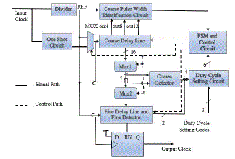
| Fig. 1(a) shows the proposed pulsewidth-controlled clock generator circuit with the adjustable duty cycle. The main building blocks are: a one-shot circuit, a coarse pulsewidth identification circuit (CPI), a coarse delay line (CDL) and a coarse detector, a fine delay line (FDL) and a fine detector, a duty-cycle setting circuit, and a finite state machine (FSM) and control circuits. The system functions are the period of the input signal is calculated by the coarse and fine delay lines, which are then recycled and controlled by the duty-cycle setting circuit to generate the final output signal with a duty cycle ranging from 30% to 66%. In the proposed pulsewidth-controlled clock generator circuit, the divider is used to divide the input clock by 2 to attain a reference signal, with a duty cycle50%, irrespective of the duty cycle of the input clock.Thus, determines the period of the input clock is equivalent to identify the REF pulsewidth. The one-shot circuit is used to generate a pulse train with a frequency corresponding the input clock, it is used only to obtain the rising edge of the output clock during the final duty-cycle setting. Initially, multiplexer (MUX) delivers REF to the CDL for the detection of pulsewidth. When the detection is completed, MUX incorporates the output of the one-shot circuit into the D flip-flop to produce the final output clock. |
 |
 |
| The pulsewidth of the input signal is determined by the CPI circuit. It also obtain the pulsewidth range of the divided REF to control the 16-to-4 MUX1 which is used to enable four output paths. For saving the power CPI circuit is used to turn off the unused coarse delay cells in the CDL, under a high-speed operation. The coarse detector has been used to compare the four MUX1 outputs with REF to select any of the 4-to-1 MUX2 input paths to enable. The fine detector is used to detect the three delay paths sequentially in the FDL to determine the delay which is closest to the REF pulsewidth. The coarse detector and fine detector operate similar to a time-to-digital converter. When the detection is completed, the same circuit is reused to determine the final output clock. The MUX output changes from REF to an output ofthe one-shot circuit to produce a pulse train. The pulse signal is then introduced into the CDL. Since the one-shot circuit can produces a signal with an equal pulsewidth without considering the input signal frequency, the input signal’s duty cycle can range from 30% to 70%. The duty-cycle setting circuit determines the obtained results from the coarse and fine detector outputs, in collaboration with the duty-cycle setting circuit input codes, and the path of the CDL, MUX1, MUX2, and the FDL can be reused to generate the final delayed output signal. A D flip-flop with asynchronous reset is used to generate the output clock. |
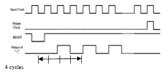
| The proposed circuit, used a pulse train, which is generated by a one-shot circuit that is passed through the CDL and FDL to obtain the desired duty cycle from the actual pulse, as evaluated by the duty-cycle setting circuit. Because we need a MUX1 and MUX2 to select the corresponding outputs of CDL and FDL.The pulsetrain signal from the output of MUX triggers the D flipflop to obtain the rising edge of the output clock. The final delay signal, which is determined by the duty-cycle setting circuit, conforms when to reset the D flip-flop to produce the falling edge of the output clock. The required value of the duty cycle can be determined from the duty-cycle setting circuit. By the use of D flip-flops implies the implementation of clocks with a small or large duty cycle at wide frequencies. The timing diagram is shown in Fig. 1 (b). The proposed circuit need a cycle to obtain the pulsewidth, and also for coarse detection, and one cycle for the duty-cycle setting circuit to obtain the final output clock signal. These detections are same for every detection and also a single cycle is required for fine detection. Then, the total operating time or locking time of the circuit is 4 cycles. These operations are achieved digitally; consequently, this methodology is easily applicable to other innovative processes. Detailed explanations of the circuit blocks are conferred below. |
| B. Design Flow Chart |
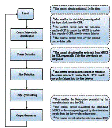
| Fig. 2.Shows the flow chart of the FSM and the process of the control circuit in each stage. Before the circuit is originally reset, the control circuit initiates all the D flip-flops. Consequently, FSM changes to the coarse pulsewidth identification state. The Mux allows the REF moves into theCDL and the CPI circuit discovers the pulsewidth range of the REF. Subsequent exposure, the control circuit enables the four outputs of the CDL into the coarse detector conferring to the detection results of the CPI circuit. The control circuit likewise turns off the idle coarse delay cells to protect power, with attention of the point that the coarse delay cells are the main source of power eating, particularly under the high-speed processes. |
| The FSMsuccessively changes to the coarse finding state, and the coarse detector then relates four outputs from the MUX1 with the REF. Following detection, MUX2 permits one path fromMUX1 into theFDL allowing to the detection results of the coarsedetector. While the FSM switches to fine detection state, the control circuit enables each path from the MUX2 to perform detection of better accuracy sequentially if the detection is not completed. After the duty-cycle setting circuit estimates the final results, the FSM changes to the output generation state. Thus, the MUX permits the pulse generated by the one-shot circuit into theCDL and D flip-flop to yield the output clock. The control circuit also re-controls MUX1 and MUX2 to enable the equivalent path to produce the desired duty cycle according to the results designed from the duty-cycle setting circuit. The control circuit instantaneously gates the REF to save power as the REF is not used for output generation. The output clock remains generating until the next reset signal. |
| A. CPI Circuit |
| CPI circuit determines the pulsewidth of REF, which is equal to the input signal period. The divided signal REF is sent to both the CPI circuit and the CDL. The CPI circuit also collects three output signals (Out4, Out8, and Out12) from the CDL. The three signals split the CDL into four parts, every parts of CDL has four coarse delay cells. The pulses of Out4, Out8, and Out12 trigger three D flip-flops in a CPI circuit, correspondingly. The pulsewidth codes F1, F2, F3, F4, and FC_FINISH are the outputs from CPI circuit and are initially set to {10000}. The CPI circuit in the proposed pulsewidthcontrolled clock generator circuit has two main tasks. First, it decreases the number of detectors needed in the CDL. Second, while the detection of the input signal is finished, the CDL, MUX1, MUX2, and FDL are recycled to generate the falling edge of the output signal. The CPI circuit turns off unused coarse delay cells to save power. |
 |
MAIN BUILDING BLOCKS |
| B. Coarse Delay Line and Coarse Detector |
| The CDL contains fifteen tri-state delay cells, C1~C15, and one matching delay cell, C16, where everyone cell has a delay of τc. The coarse delay line is separated into four groups: C1~C3, C4~C7, C8~C11, and C12~C15. MUX1 enables one signal of each group into coarse detector to detect the period of input clock. If the pulsewidth of the input signal REF is larger than 8τc and smaller than 12 τc, the CPI circuit identifies it and produces output codes F1~F4 of {0010}, and points MUX1 to enable the 4 outputs (Out8~Out11) of delay cells C8~C11. Because C12~C15 delay cells are not used and it is the turns off CPI circuit to save power. After the detection is complete, the control circuit decides which of the MUX2 paths to enable and pass to the fine delay block for more precise detection. |
| C. Fine Delay Line and Fine Detector |
| The FDL comprises three tri-state delay cells. Every cell has a delay ����, which, is equal to one fourth of τc. In the conventional structure detectors, every delay cell is connected to a D flip-flop for phase detection, a subsequent delay cell, and an output buffer, which is related to the structure of the coarse detector. To develop the time resolution of the fine delay line, a serial structure is used to invent the fine detector. Altered a parallel structure, a serial structure permits the fan-out of the delay cells to bediminished.since phase detection is only achieved on the last delay cell, instead of on all of them. Since signal Input_fine is resulting from the coarse delay line, the phase difference between Input_fine and REF is smaller than the delay time of one coarse delay cell. By using only three delay cells, the fine delay line not only decreases detection time, but also increases the time resolution. |
| D. Duty Cycle Setting Circuit |
| Fig. 3 shows the proposed duty-cycle setting circuit. Identified results of the coarse detector and fine detector are converted to 6-bit binary code (bits [4:9]) by the thermometer-to-binary encoder. The binary code is then sent to the dutycycle setting circuit, which Determines the corresponding |
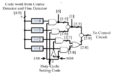 ' ' |
| resultbased on the duty-cycle setting codes delivered by the user.Because the identified digital code corresponds to the period of the input signal, an output clock with the preferred duty cycle can be implemented by sending the pulse with the desired delay, to reset the D flip- flop of the output clock generator. For example, because the detected digital codes correspond to a 100% duty cycle, a 50% duty cycle output clock can be realized by dividing the detected digital codes by 2. In addition, 25%, 12%, and 6% duty cycles can be realized by sending the pulse with the desired delay, to reset the D flip- flop of the output clock generator. |
| For example, because the detected digital codes correspond to a 100% duty cycle, a 50% duty cycle output clock can be implemented by dividing the detected digital codes by 2. In addition, 25%, 12%, and 6% duty cycles can be attained by dividing the detected digital codes by 4, 8, and 16, correspondingly. The implementation of the duty-cycle setting circuit uses shift registers to express the division of the code: one shift corresponds to 1/2; two shifts correspond to 1/4; and so on. The duty cycle setting circuit then adds the codes to generate the final results using full adders controlled by the setting codesin our design, becauseand do not appear concurrently, hardware cost can be reduced by having two codes share an addition operation. |
SIMULATION AND EXPERIMENTAL RESULTS |
| A. Experimental Results |
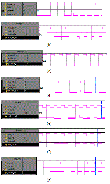
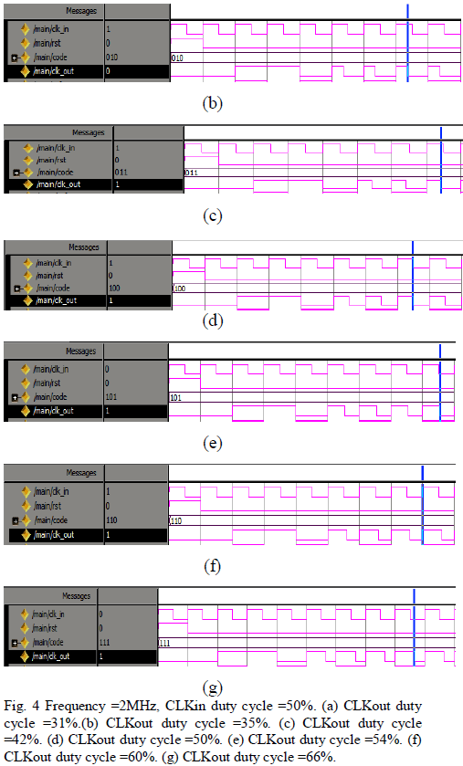
| The proposed circuit was implemented using the 0.18-μm CMOS Technology. The interconnects area is of 4.093778 and the operating frequency range is 2 MHz. Fig. 4 shows the output waveforms of duty cycles ranging from 31% to 66% at 2 MHz. Our results indicate that the proposed duty cycle setting circuit can operate correctly across a range of frequencies and generate correct outputs for the corresponding duty cycles with the locking time of 4 cycles. We adopted the structure of an inverter chain in the output driver of the proposed circuit by increasing the size of the inverter at each stage by a factor of two to three to drive the parasitic loads of the bonding pads and the output measurement equipment. |
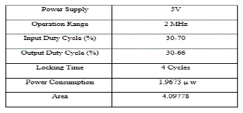 |
| Although the inverter chain is used to drive the loading, when the signal first arrives in the inverter chain, the parasitic inductance of the bonding wire influences the stability of the output clock for several clock cycles. The output clock stabilizes afterwards. Power consumption is 1.9673μW. The performance summary and comparison are provided in Tables I and II, respectively. |
 |
 |
CONCLUSION |
| Many systems, such as DDR-SDRAM and doublesampling analog- to-digital converter, use the rising and falling edges of the reference clock signal to sample the input signal. Differences in process, voltage, and temperature (PVT) may impact the duty cycle of the clock signal, making it difficult to regulate the duty cycle precisely at 50%. As a result, a number of pulsewidth-control loops (PWCLs) have been proposed to overcome this deviation of high-speed operations. In this paper a pulsewidth-controlled clock generator circuit with programmable duty cycle is presented. The proposed approach using two delay lines and a time-todigital detector is capable of reducing hardware costs, compared with previous solutions, while achieving an equal degree of accuracy. A newduty-cycle setting circuit is proposed to produce output duty cycles from 30% to 66% without the need for a look-up table. The operating frequency of this circuit ranges from 2 MHz with an input cycle range from 30% to 70%. The circuit has interconnects area of 4.093778, provides fast locking (4 cycles) of the DLL. |
ACKNOWLEDGEMENT |
| The authors acknowledge the contributions of thestudents, faculty of Velalar College of Engineeringand Technology for helping in the design of testcircuitry, and for tool support. The authors alsothank the anonymous reviewers for theirthoughtfulcomments that helped to improve this paper. Theauthors would like to thank the anonymousreviewers for their constructivecritique from whichthis paper greatly benefited. |