International Journal of Innovative Research in Science, Engineering and Technology
ISSN ONLINE(2319-8753)PRINT(2347-6710)
ISSN ONLINE(2319-8753)PRINT(2347-6710)
R.Umamageswari, T.A.Raghavendiran
|
| Related article at Pubmed, Scholar Google |
Visit for more related articles at International Journal of Innovative Research in Science, Engineering and Technology
Multilevel inverter becomes popular because of its high power, high voltage application. However it has some disadvantages such as increased number of components, complex control method and voltage balancing problems. In this paper, we proposed a new topology having level modules and H-bridge inverter, and reverse voltage technique is adopted for load. APOD based PWM technique is used to generate pulses for switches. This method requires less components for operation and THD is reduced to a greater level. For voltage THD is 8.12% and for current THD is 0.53.Simulation is done using SIMULINK/MATLAB software. Index terms’-bridge inverter, multilevel module, THD
INTRODUCTION |
| Increase in demand of Electricity leads to the use of renewable energy sources such as solar, wind etc. In case of solar energy is harnessed in the form of dc. This DC is converted into AC and fed to grid or ac loads. In recent years there was increase in demand for multilevel power conversion. Research has involved the introduction of novel converter topologies and unique modulation strategies. However, the most recently used inverter topologies, are cascade inverter, neutral-point clamped (NPC) inverter, and flying capacitor inverter. Our proposed topology consists of level module and HBridge inverter and they are connected in parallel. Proposed topology is symmetric topology since the values across all the DC sources are same. However, there are asymmetrical topologies which require different voltage sources. This criterion needs to arrange dc power supplies according to a specific relation between the supplies. Difference in ratings of the switches in the topology is also a major drawback of the topology. This paper presents an overview of a new multilevel inverter topology named reversing voltage RV). This topology requires less number of components compared to conventional topologies. It is also more efficient since the inverter has a component which operates the switching power devices at line frequency. |
| Therefore, there is no need for all switches to work in high frequency which leads to simpler and more reliable control of the inverter. In this topology 15level output voltage is produced. |
II. NEW MULTILEVEL TOPOLOGY |
| In conventional multilevel inverters, the power semiconductor switches are combined to produce a highfrequency waveform in positive and negative polarities. However, there is no need to utilize all the switches for generating bipolar levels. This idea has been put into practice by the new topology. This topology is a hybrid multilevel topology which separates the output voltage into two parts. One part is named level generation part and is responsible for level generating in positive polarity. This part requires high-frequency switches to generate the required levels. The switches in this part should have high-switching-frequency capability. The other part is called polarity generation part and is responsible for generating the polarity of the output voltage, which is the low-frequency part operating at line frequency. |
| The topology combines the two parts (high frequency and low frequency) to generate the multilevel voltage output. In order to generate a complete multilevel output, the positive levels are generated by the high-frequency part (level generation), and then, this part is fed to a full-bridge inverter (polarity generation), which will generate the required polarity for the output. This will eliminate many of the semiconductor switches which were responsible to generate the output voltage levels in positive and negative polarities. |
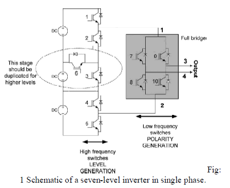 |
| In fig 1, left side multilevel module generates the required output level without polarity and right side HBridge decides the polarity of output voltage and current. This topology requires fewer components in comparison to conventional inverters. Another advantage of the topology is that it just requires half of the conventional carriers for SPWM controller. The reason is that, according to Fig. 1, the multilevel converter works only in positive polarity and does not generate negative polarities. Therefore, it implements the multilevel inverter with a reduced number of carriers, which is a great achievement for inverter control. It is also comparable to single-carrier modulation, while this topology requires the same number of signals for PWM. |
III.PWM TECHNIQUE |
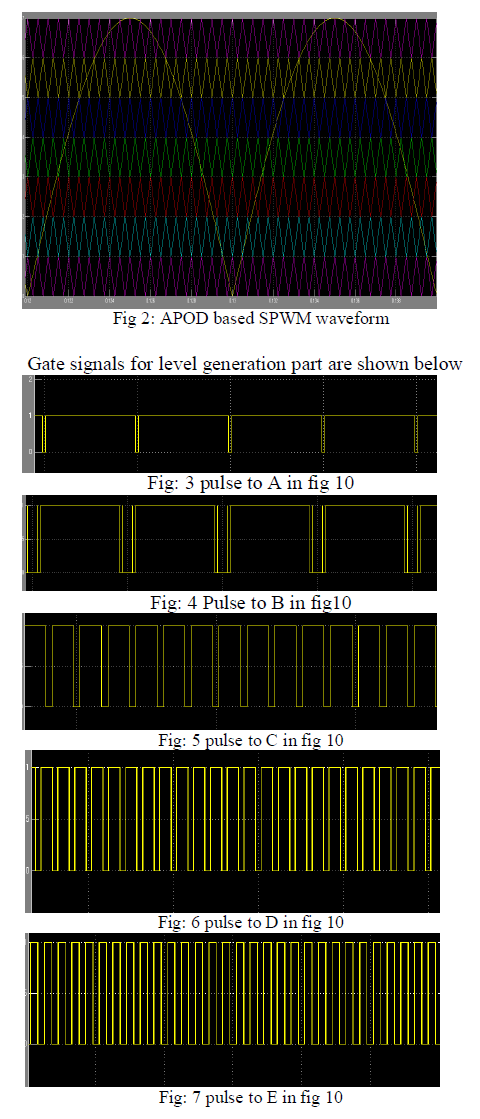
| In this paper we used the alternative phase opposition disposition scheme. In APOD all the carriers are phase opposition by 180 degree from its adjacent carrier as shown in fig. 2. |
 |
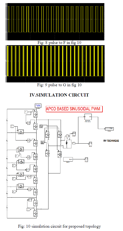 |
| Simulation circuit using simulink is shown in the fig 10. In that left side 14 switches are used for generating level of output voltage (high frequency switches).Right side 4 switches are used for polarity generation (low frequency switches). No of switches used 18 and is calculated by |
| S= (n-1) +4 |
| Where |
| n- no of level required. |
| s-no of switches used. |
| RL load is connected across the H-Bridge inverter R=115Ω, L=182mH. |
V.SIGNAL GENERATION CIRCUIT |
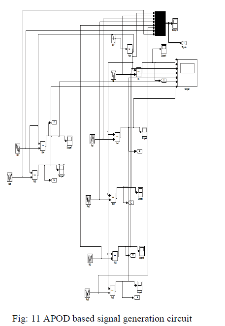 |
| Operation-In the output voltage, positive cycle is generated by first 7 switches in the left side level module and 4 switches in the right side H-Bridge inverter. Whereas negative cycle is generated by next 7 switches in left side level module and 4 switches in the right side H-Bridge. |
| In fig11, reference wave (sine wave) and carrier wave (ramp) modulated to generate the pulses for switches and each carrier is 180âÃâæ out of phase. |
 |
VI.SIMULATION RESULTS |
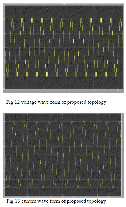
| In Fig 12 shows the voltage wave form of proposed system. Output voltage is equal to the sum input DC voltages |
 |
VII.THD CALCULATION |
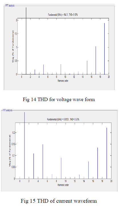
| THD is calculated using FFT analysis in SIMULINK/MATLAB. THD is calculated for 30 cycles with the fundamental frequency of 50HZ. |
| Fig 14 shows THD value of output voltage. The value of THD for output voltage is found to be 8.12%.Fig 15 shows the THD value of output current. The value of THD for output current is found to be 0.54% |
 |
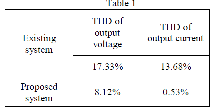 |
| Table 1 shows the comparision between existing system and proposed system THD for output voltage and current. |
VIII.CONCLUSION |
| In this paper new topology has been proposed which has superior features over the conventional topologies reduced no of switches are used .The switching operation is separated into high- and lowfrequency parts. This will add up to the efficiency of the inverter as well as reducing the size and cost of the final prototype. The APOD-SPWM control method is used to drive the inverter. The PWM for this topology has fewer complexities since it only generates positive carriers for PWM control. Simulations are done using SIMULINK/MATLAB. |
References |
|