This paper presents a resonant SEPIC (Single-Ended Primary Inductor Converter) Converter and Control method suitable forVery High Frequency dcdc Power Conversion. SEPIC is chosen since it has positive voltage gain and higher characteristics than any other converter. The proposed design provides high efficiency over a wide range of input and output voltage ranges, up & down voltage conversion, small size and excellent transient performance. The Converter regulates the output using an ON-OFF control scheme modulating at a fixed frequency and duty ratio operation. This control method enables a fast transient response and efficient light-load operation while providing controlled spectral characteristics of input and Output waveforms. The resonant inductors and capacitors are fine tuned to achieve Zero Voltage Switching (ZVS) condition and thus the converter achieves higher than 80% efficiency across entire input voltage range at nominal output voltage and maintains good efficiency across the whole operating range.
Keywords |
| SEPIC Converter, ON-OFF control
strategy, PID Controller, Zero Voltage Switching. |
INTRODUCTION |
| Probably most of the electronic applications could
benefit from a Power Converter and it is capable to
achieve high efficiency across wide input and output
voltage ranges at a small size. Although it is difficult for
many conventional power converter design to provide
wide operation range while maintaining high efficiency,
especially if both up & down voltage conversion is to be
achieved[2]-[4]. Furthermore, High energy storage
required at contemporary switching frequencies of a fewmegahertz and below, limits the degree of contraction
that can be achieved and obstructs fast transient response.
Therefore, design methods that reduce energy storage
requirements and expand efficient operation range are
desirable. In this paper, we exploit the use of resonant
switchingalong with fixed frequency control techniques
to achieve these goals. |
| DC-DC converters are used in power supply circuits
forstabilizing the voltage to any desired value [1]. SEPIC
(Single Ended Primary Inductor Converter) converter is a
fourth-order nonlinear system and it is extensively used in
step-down or step-up dc-dc switching circuits and PFC
(Power Factor Correction) circuits because it has several
characteristics: |
| 1) The same polarity between input and output voltage |
| 2) Small input ripple current |
| 3) Step-down and Step-up operation |
| 4) Easily extended to multiple-output |
| Power electronic circuits are rich in nonlinear
dynamics. Their operation is characterized by cyclic
switching of circuit topologies, which gives rise to a
variety of nonlinear behaviour. |
| This paper introduces a quasi-resonant single-ended
primary inductor converter (SEPIC) converter [1], [7]
resonant switching and associated control method suitable
for converter design at frequencies above 2MHz. Unlike
many resonant converter designs the proposed approach
provides high efficiency over very wide input and output
voltage ranges and power levels. It also provides up-anddown
conversion, and requires little energy storage which
allows for tremendous transient response. Unlike
conventional quasi-resonant and multiresonant converters
no bulk inductor which reduces the Electro Magnetic
Interference and the converter operates at fixed frequency and duty ratio. These aspects reduce passive component
size & progress response speed. A new fixed-frequency
ON/OFF control is introduced which provides good
control over input and output frequency content. Section
II presents the Design of SEPIC converterand discusses
its mode. Modelingof converterand tuning of the
controller are explained in detail in Section III, followed
by the discussion of Soft Switching in Section IV. Section
V presents the design and simulation result and
Conclusion is presented in Section VI. |
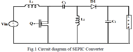
II. DESIGN OF SEPIC CONVERTER |
| A Single Ended Primary Inductor converter (SEPIC)
is a dc – dc converter, whose output voltage can be
controlled by the duty cycle of the switching device. The
circuit diagram of the SEPIC converter is shown in Fig. 1.
The SEPIC converter consists of a switch (S) with duty
cycle d, a diode (D1), two inductors (L1 and L2), two
capacitors (C1 and C2) and a resistor load (R). For
simplicity, R load is used here. As per the application
required load can be varied and the response can be
obtained. All the elements are assumed to be ideal and
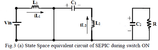
assuming the conduction to be continuous. The equivalent
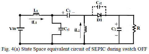
circuits during switch ON and OFF states are shown in |
| Fig. 2(a) and Fig. 2(b) also the design of SEPIC is
done. |
 |
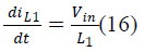
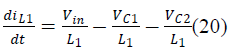
| When Q turns ON, the energy is stored in the inductor
L1. At this time the inductor voltage equals to input
voltage, and the energy stored in capacitor C1 will be
transferred to inductor L2. The load is supplied by
capacitor C2 as shown in Fig.2 (a). |
 |
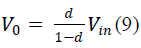
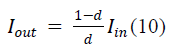
| Applying KVL, |
| Considering L1, |
 |
| Considering L2, |
 |
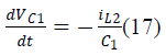
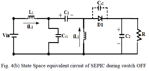
| As shown in Fig.2 (b) When Q turns OFF, the energy
stored inInductor L1 is transferred to C1. The energy
stored in L2 is transferred to C2 through D1 and
supplying the energy to Load. |
 |
| Applying KVL, |
| Considering L1, |
| We know that, V0=VC2 |
 |
| Considering L2, |
 |
| Average Voltage across L1& L2 is Zero. So, |
 |
 |
| Equation (6) becomes, |
 |
| Averaging the equations (9) & (2) to zero, |
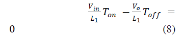 |
| We Know that, |
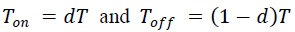 |
| By simplifying the above expression we get,
The average output Voltage is |
 |
| For the lossless Circuit, |
 |
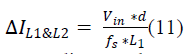
| The peak-to-peak ripple current in the inductor L1 & L2 |
 |
| According to the variation in duty cycle d, this SEPIC
converter acts as either buck or boost converter. |
III. MODELING OF SEPIC CONVERTER |
| Modeling of a particular converter is done by either
Circuit Averaging Method or State Space Averaging
method. Here State Space Averaging method is used for
modeling of SEPIC converter. It is an approximation
technique thatapproximates the switching converter as a
continuous linear system.State Space Averaging requires
that the effective filter corner frequency fc smaller than
the switching frequency fs. The Power stage of closed
loop system is a non-linear system. The non-linear
systems are usually difficult to model and are also
difficult topredict the behaviour of the non-linear system.
So, it is better to approximate the non-linear system to a
linear system. For the linearized power stage of dcdcconverter
Bode plot can be used to determine
suitablecompensation in feedback loop for desired
steadystate and transient response. For this the State
SpaceAveraging technique is used. |
| In dc-dc converter operating in CCM has two circuit
states: one when the switch is turned ON and other when
the switch is turned OFF. |
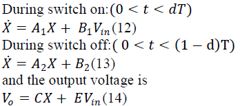 |
| To produce an average description of the circuit over a
switching period, the equations corresponding to the two
foregoing states are time weighted andaveraged, resulting
in the following equations: |
 |
| Where, |
| ‘d’ is the duty cycle of the switch. |
 is the electric charge. is the electric charge. |
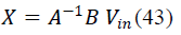
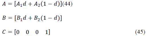
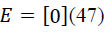
| A is thesystem matrix of the converter |
| B is the input matrix of the converter |
| C is the Output matrix of the converter. |
| E is the direct transmission matrix of the converter |
| This equation shows that by controlling the duty cycle of
the switch the output voltage Vo can be controlled and
output voltage can be high or low or equal to the input
voltage Vin. The duty cycle of the SEPIC converter can be
varied during operation by using a controller and the
circuit can also be made to reject disturbances. |
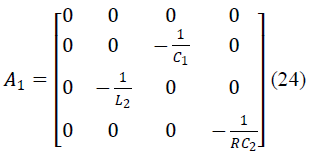
| A. State Space Averaging of Conventional SEPIC Converter |
| The state space equations for SEPIC converter during
switch ON and OFF are |
| During switch ON: |
 |
 |
 |
 |
 |
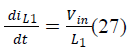
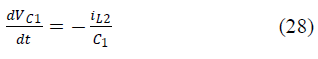
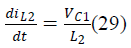
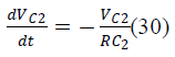
| During Switch OFF: |
 |
 |
 |
 |
 |
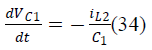
| And states of the SEPIC converter are iL1, iL2,VC1,VC2.
The averaged matrices for the steady-state and linear
small-signal state-space equations can be written
according to above equations. |
 |
 |
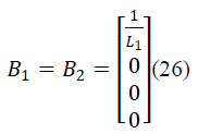 |
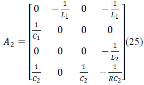
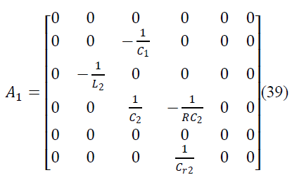
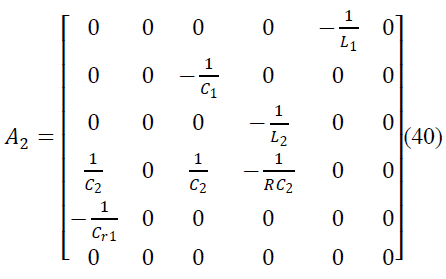
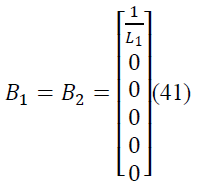
| B. State Space Averaging of Proposed SEPIC Converter |
| The state space equations for SEPIC converter during
switch ON and OFF are |
| During switch ON: |
 |
 |
 |
 |
 |
 |
 |
| During switch OFF: |
 |
 |
 |
 |
 |
 |
 |
| iL1, iL2,VC1,VC2, VCr1, VCr2 are the state variables of
SEPIC converter. The averaged matrices for the steadystate
and linear small-signal state-space equations can be
written according to above equations. |
 |
 |
 |
| C. Transfer Function Evaluation |
| With the state space matrices defined above, the
transfer function is given by, |
 |
 |
| Where, |
 |
| For Conventional SEPIC |
| and |
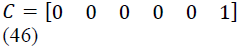 |
| for Proposed resonant SEPIC |
 |
| After discovering the values of A, B, C & E evaluate
them toobtain the transfer function. Compute Kp, Ki&Kd
parameters to tune the controller. |
| Where, |
| Gvv – Transfer function. |
| Kp- Proportional gain; of the controller. |
| Ki – Integral gainof the controller. |
| Kd- Derivative gain; of the controller. |
| D. Controller Tuning |
| PID controllers use a 3 basic behaviour types or
modes: |
| P - Proportional, I - Integral and D - Derivative. While
proportional and integral modes are also used as single
control modes, a derivative mode is rarely used on its
own in control systems. Combinations such as PI and PD
control are very often in practical systems. |
 |
| When P controller is used, large gain is needed to
improve steady state error. |
| D mode is used when prediction of the error can improve
control or to stabilize the system. Sudden
change in error signal will cause sudden change in
control output. |
| PI controller will eliminate forced oscillations and
steady state error and introducing integral mode has a
negative effect on speed of the response and overall
stability of the system. |
| PID controller has all the necessary dynamics: fast
reaction on change of the controller input (D mode),
increase in control signal to lead error towards zero (I
mode) and suitable action inside control error area to
eliminate oscillations (P mode). |
| Derivative mode improves stability of the system and
enables increase in gain K and decrease in integral
time constant Ti, which increases speed of the controller
response. PID controller is often used in industry,
but also in the control of mobile objects. |
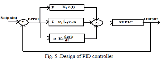
| So, in this paper closed loop analysis of SEPIC Converter
is done by PID controller since it can be used in dealing
with higher order capacitive processes. Fig.4 shows the
plant modelof the controller which uses PID for execution
and also better response will be produced since its higher
order controller.. For PID tuning various methods have
been used,paper Cohen-Coon tuning method is used
which is duly used for stiff system. |
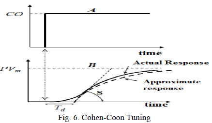
| E. Cohen-Coon Tuning Method |
| This technique was proposed by G.H.Cohen and
G.A.Coon. The process output is affected not only by the
dynamics of the main process but also by the dynamics of
the measuring sensor and final control element. They
observed that the response of most processing unit to an
input changehad a sigmoidal shape and it is shown in
Fig.5. |
 |
| Where, the transfer function is given by |
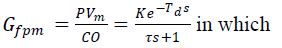 |
 |
 S is the slope of the sigmoidal response of the
Inflection. S is the slope of the sigmoidal response of the
Inflection. |
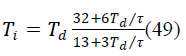
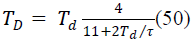
| Td = Time elapsed until the system responded. |
| From the obtained steady state response we have to
compute the parameters Kp,Ki&Kd using these
expressions given below. |
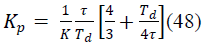 |
 |
 |
| The Transfer function of PID controller is given by: |
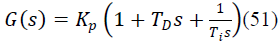 |
| Where, |
| Kp = Proportional gain. |
| TD = Derivative time constant. |
| Ti = Integral Time Constant. |
| K = the output steady state divided by the input step
change, |
| τ = the effective time constant of the first order response, |
| Td = the dead time(time elapsed until thesystem
responded). |
| By this above mentioned method initial tuning was done
and to get a well-tuned controller output, fine tuning must
be done manually as a further progress. |
IV. SOFT SWITCHING OF CONVERTER |
| Conventional PWM power converters were operated
in a switched mode operation. There are two types of
switching namely, |
| a. Hard Switching |
| b. Soft Switching |
| Hard switching refers to stressful switching behaviour of
the power electronic devices.During the turn-ON and
turn-OFF processes, the power device has to withstand high voltage and current simultaneously, resulting in high
switching losses and stress. Capacitive snubbers are used
to limit the stress |
| However; the switching loss is proportional to the
switching frequency, thus limiting the maximum
switching frequency of the power converters. |
| In order to reduce the switching loss soft-switching
techniques are used (i.e.) Resonant converter is
incorporated. Two techniques namely ZVS(Zero Voltage
Switching) and ZCS(Zero Current Switching) are used for
Turn-ON and Turn-OFF transition of the switch. Tank
circuits (L&C) are tuned to obtain these switching which
results in increase in switching frequency of the
converter, continuous improvement of the switch and
reduction in switching loss gradually increase the
efficiency of the converter. |
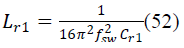
| A. Proposed Soft Switching Technique |
| In this paper (Zero Voltage switching) ZVS condition
is obtained during Turn-ON Transition of the switch. This
proposed resonant SEPIC converter is the combination of
both quasi resonant SEPIC and Multiresonant SEPIC
converter. Multi resonant uses bulk inductors, introduces
capacitance in parallel with switch and diode, quasi
resonant uses choke inductor Lr1 along with coupling
capacitor Cs to achieve ZVS condition. Combination as
Quasiresonant and multi resonant technique ensures fixed
frequency and duty ratio operation which eliminates the
bulk magnetic component and enables ZVS which
increases the efficiency of the converter. The proposed
Resonant SEPIC converter is shown in Fig.6. In this new
resonant SEPIC converter no bulk inductor is used, two
resonant inductors and capacitors used namely, |
| a. Lr1and Cr1 |
| b. Lr2and Cr2 |
 |
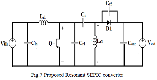 |
| Resonant inductor Lr2 and Capacitance Cr1 and Cr2 are
tuned approximately to deliver the output. First, design
the open loop SEPIC converter and find all the
parameters required. Further for achieving resonant
condition introduce capacitance in parallel with diode and
switch and tune them particularly to get a specified
output. |
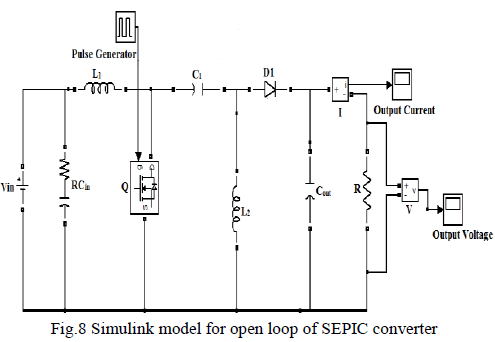
V. SIMULATION RESULTS |
| In order to verify the proposed topology of the
resonant switching of the SEPIC converter the simulation
results have been analyzed by open loop and closed loop
model of SEPIC converter and also by the comparative
analysis of Conventional and proposed SEPIC. For closed
loop model, PID controller parameters have been
calculated using Cohen-Coon Technique explained in
Section III.D. The simulations have been done by
MATLAB/Simulink.The parameters are |
| For Conventional SEPIC: |
| Vin or Vdc =3.6V, L1=L2=64.89μH, |
| C1=10μF, C2=39.144nF, Dmax =56%. |
| For resonant SEPIC: |
| Lr1=Lr2= 64.89μH, Cr1= 3.8pF; Cr2=20nF, CS=10μF and it |
| is well tuned for better response. |
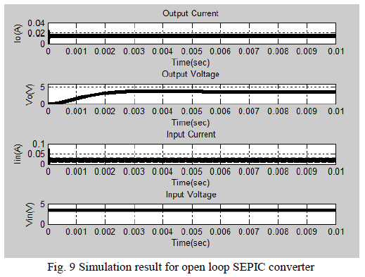
| A. Open LoopModelfor SEPIC Converter |
 |
 |
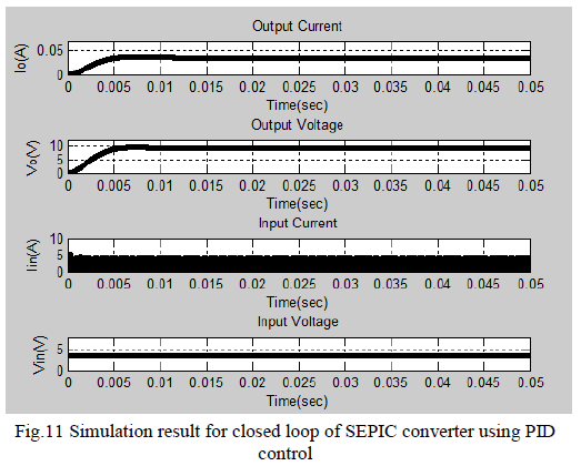
| B. Closed Loop Modelfor SEPIC Converter |
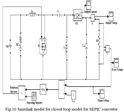 |
 |
| C. Proposed Resonant SEPIC Converter Model |
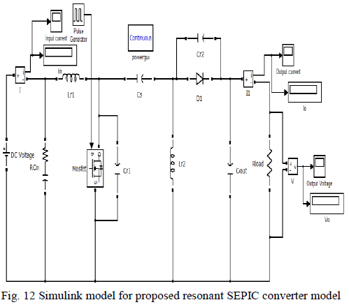 |
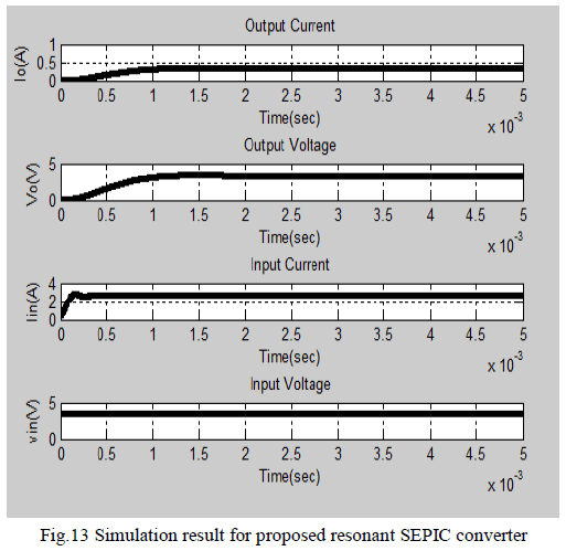 |
| D. Proposed Closed loop ofResonant SEPIC converter |
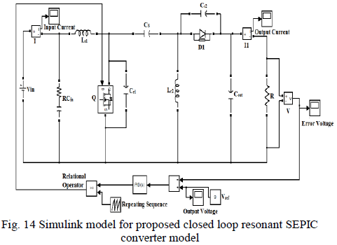 |
 |
| E. Comparative Efficiency Analysisof SEPIC Converter |
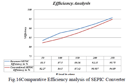 |
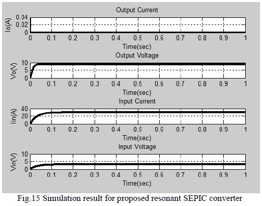
| From the abovesimulation results we examine the
response of SEPIC converter for Open loop analysis in
Fig.8, Closed loop analysis in Fig.10 and the proposed
resonant SEPIC analysis in Fig.12. Also the comparative
efficiency analysis had been done and verified through
the graph shown in Fig.13. The graph implies that
resonantSEPIC have higher efficiency compared to
conventional SEPIC due to Zero Voltage Switching
condition achieved in it. It is obtained by tuning the
resonant circuit includes inductors (Lr1 & L r2) and
Capacitors (Cr1 & Cr2) as shown in Fig.6. The variations
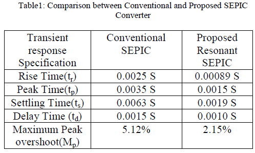
are compared as shown in Table1. |
 |
VI. CONCLUSION |
| This work presents a resonant SEPIC converter suitable
for extremely high-frequency operation and for operating
across a wide input and output voltage range. Here
we experimentally set up a SEPIC converter with switching
frequency MHz.This work uses an ON-OFF control
with fixed frequency. It is possible for resonant SEPIC
converters to achieve a wide operating range, a small size,
and excellent transient response while maintaining good
efficiency. It provides fast transient response and good
control over wide input and output ranges. In this we can eliminate the bulk magnetic components and facilitates
high efficient resonant
Gating. Soft switching can be achieved for a wide input
and output voltage ranges. |
| Unlike conventional quasi- resonant and multi
resonant converters no bulk inductor is used and the
converter operates at fixed frequency and duty ratio.
These attributes reduce passive component size, improve
response speed, and enable the use of low-loss sinusoidal
resonant gating. It is hoped that these techniques will
contribute to future development of low-power converters
operating over wide ranges and extreme high frequencies
to meet the increasing demands of modern portable
electronics. |
References |
- J. Hu, A. D. Sagneri, J. M. Rivas, S. M. Davis, and D. J. Perreault,“High frequency resonant sepic converter with wide inputand output voltage ranges,” in Proc. IEEE Power Electron. Spec.Conf., Jun. 2008, pp. 1397âÃâ¬Ãâ1406.
- J. M. Rivas, “Radio frequency dc-dc power conversion,” Ph.D.dissertation, Dept. Elect. Eng. Compute. Sci., Massachusetts Instituteof Technology (MIT), Cambridge, Sep. 2006.
- J. Perreault, J. Hu, J. M. Rivas, Y. Han, O. Lietermann, R. Pilawa,A. Sagneri, and C. Sullivan, “Opportunity and challenges invery high frequency power conversion,” in Proc. 24th Annu.IEEE Appl. Power Electron. Conf. Expo., 2009, pp. 1âÃâ¬Ãâ14.
- J. R. WarrenIII, K. A. Rosowski, and D. J. Perreault, “Transistorselection and design of a VHF dc-dc power converter,” IEEETrans. Power Electron., vol. 23, no. 1, pp. 27âÃâ¬Ãâ37, Jan. 2008.
- J.Rivas, D.Jackson, O.Leitermann, A.Sagneri, Y.Han and D.Perreault,“Design Consideration for very high frequency dc-dc converters,”in proc Power Electron.Spec.conf. Jun.18-22, 2006,pp.1-11.
- J.Rivas, R.Wahby, J.Shafran and D.Perreault, “New architecturesfor radio frequency dc/dc power conversion,” IEEE Trans.Power E
- lectron. vol.21, no.2, pp.380-393, Mar.2006.
- R.Erickson and D.Maksimovic, “Fundamentals of Power ElectronicsâÃâ¬ÃÂ,Norwell, MA: Kluwer, 2000.
- Ray Ridley, “Analyzing the Sepic Converter”, Power SystemsDesign Europe, November, 2006, pp. 14-18.
- Tae-Yeong Lee, Eun-JuYoo, Won-Yeong Choi, and Young-WooPark, “Design and Control of DC-DC Converter for the MilitaryApplication Fuel Cell” IEEE Appl., World Academy of Science,Engineering and Technology 47 2010.
- W.Tabisz and F.Lee, “Zero Voltage-Switching multiresonanttechnique: A novel approach to improve performance of Highfrequency quasi resonant converters,” IEEETrans.PowerElectron., vol.4no.4, pp.450-458, Oct 1989.
- Wei Gu, Dongbing Zhang, “Designing a SEPIC Converter”,Excellent Design Guidelines, National Semiconductor in ApplicationNote, April, 2008, pp. 1-6.
- Y. Han and D. J. Perreault, “Analysis and design of high efficiencymatching networks,” IEEE Trans. Power Electron., vol.21, no. 5, pp. 1484âÃâ¬Ãâ1491, Sep. 2006.
- Y.Lee and Y.Cheng, “A580KHz switching regulator using on offcontrol,”J.Inst.Electron. RadioEng. vol.57, no.5pp.221 -226,Sep/Oct.1987
|