International Journal of Innovative Research in Science, Engineering and Technology
ISSN ONLINE(2319-8753)PRINT(2347-6710)
ISSN ONLINE(2319-8753)PRINT(2347-6710)
| Bushra. K.H.al-Maiyaly, I.H.Khudayer1, Ayser.J.Ibraheim1 Associate Professor, Department of Physics, College of Education for Pure Science / Ibn Al-Haitham, University of Baghdad, Baghdad, Iraq. |
| Related article at Pubmed, Scholar Google |
Visit for more related articles at International Journal of Innovative Research in Science, Engineering and Technology
The structural, optical properties of copper oxide thin films ( CuO) thin films which have been prepared by thermal oxidation with exist air once and oxygen another have been studied. Structural analysis results of Cu thin films demonstrate that the single phase of Cu with high a crystalline structure with a preferred orientation (111). X-ray diffraction results confirm the formation of pure (CuO) phase in both methods of preparation. The optical constant are investigated and calculated such as absorption coefficient, refractive index, extinction coefficient and the dielectric constants for the wavelengths in the range (300-1100) nm
Keywords |
| Copper Oxide, Thin Films, Optical Properties, Structural properties, Thermal Evaporation. |
INTRODUCTION |
| Copper Oxide (CuO) material is known p-type semiconductor in general which useful for constructing junction devices such as pn junction diodes [1] , [1] , having a relatively low band gap (1.3-2.1) eV with monoclinic structure [1,2]. Copper Oxide has been studied as a semiconductor material because of natural abundance of starting material (Cu); low cost production processing; non-toxic nature; and reasonably good electrical and optical properties [3]. Apart from this semiconductor applications, this material (CuO) has been studied for photoconductive and photo-thermal applications, it has attracted much interest in recent years because it is the basis of several high-Tc super conductors [3,4]. Copper Oxides have been used as electrode materials for lithium batteries, in addition to photovoltaic devices [5]. CuO composites such as CuO-ZnO and CuO-SnO2 systems also find applications in humidity and gas sensors [6,7]. CuO nanowires can also be used in p-type field effect transistors [8]. Several methods of deposition techniques have been used to prepare Copper Oxide films (CuO), such as thermal evaporation [9], electro deposition [10], chemical vapor deposition [11], spray pyrolysis [12], plasma evaporation [13], pulsed laser deposition [14], molecular beam epitaxy [15], and sol- gel techniques [16] etc. In this research the thermal evaporation technique was used to preparation (Cu) thin films and then oxidation these films to get (CuO) films. |
EXPERIMENTAL |
| Copper pure metal thin films have been deposited on glass substrate by thermal evaporation technique in a high vacuum system of (3x10⁻⁶) torr using Edward coating unit model (E 306) from molybdenum boat, the distance between the boat and substrate was about 15 cm. Films thickness was about (500±50) nm at R.T (300 K) with deposition rate (1.1 nm/sec). The thermal oxidation processes were carried out on these films at temperature of (773) K for one hour by using (Kilns Furnaces) with exist air flow once, and oxygen gas at rate flow (500 sccm) in another time. The effect of exist two different gases during prepared (CuO) films on the structural and optical properties of these films has been studied. The structure of the Cu and CuO thin films has been examined by X-ray diffraction method (XRD) using siemens x-ray diffractometer system, which records the intensity as a function of Bragg angle., at the following operation condition-:Source Cu Kα radiation of wavelength (λ=1.5405 æ), -Current =20mA, Voltage =4kV, -Scanning speed = 5 cm/min, We can get information about the crystal structure such as phase crystalline, polycrystalline, amorphous, grain size, and lattice parameter. The inter planer distance d (hkl) for different planes was measured by Bragg's law: |
 |
RESULTS AND DISCUSSION |
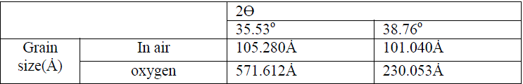
| We can deduce from the X-ray diffraction pattern in figure (1) that the thin films have polycrystalline structure. Part (A) of the figure show that the Cu thin films has single phase of Cu with high a crystalline structure with a preferred orientation (111) at 2ÃÂ=43.723o at, and small peaks belong also to Cu phase at (2ÃÂ=50.897 and 74.52o), with orientation at (220) direction. Parts (B and C), show the X-ray diffraction pattern of CuO thin films, part (B) present the CuO films that oxidation in air, and part (C) for the films that prepared in oxygen ambient. Results confirm the formation of pure CuO phase at (2ÃÂ=35.53 and 38.76o), with a preferred orientation at (111). From part (B and C), we notice that the intensity of CuO thin films that oxidation in oxygen ambient becomes stronger and sharper than that which has been oxidized in air due to the improvement of the crystallinity in the films. The drain size calculated using equation (5) increase when we use oxygen ambient, which was demonstrated the improvement of the crystallinity in the films, as shown in table I. Figure (2) shows the variation of absorbance (A) versus wavelength of CuO thin films prepared, we can see from this figure the absorbance values decreased generally with wavelength and has low values in the NIR region. A strong absorption at wavelength range of (300-410) nm, which is made Copper Oxide films suitable for solar cell. It is clear from this figure that the absorbance values increases when we used oxygen flow for oxidation processes. The variation of the transmittance with wavelength of CuO thin films is shown in figure (3), from this figure we can notice that the transmittance increase with wavelength and have high transmittance in the NIR region, which makes these films suitable for solar energy collection. Also we can see from this figure the transmittance values decreased when we used oxygen flow for oxidation processes. |
| Table 1. Present the changing of grain size with method of preparation |
 |
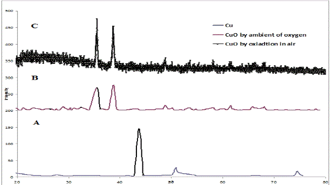 |
| Fig. 1 presents the X-ray diffraction pattern of CuO |
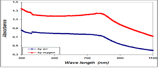 |
| Fig. 2 The variation of absorbance versus wavelength for copper oxide thin films |
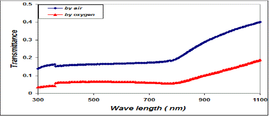 |
| Fig. 3 The variation of transmittance versus wavelength for copper oxide thin films |
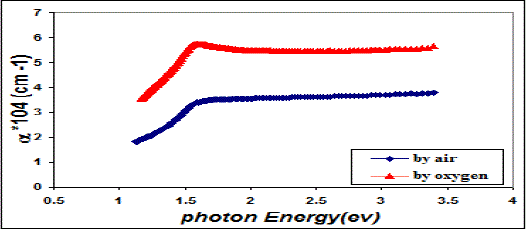 |
| Fig. 4 Absorption coefficient as a function of photon energy for CuO thin films |
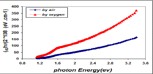 |
| Fig. 5 Variation (α hν)2 & photon energy for copper oxide thin films |
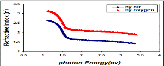 |
| Fig. 6 Variation refractive index & photon energy for copper oxide thin films |
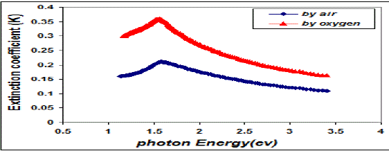 |
| Fig. 7 Variation extinction coefficient & photon energy for copper oxide thin films |
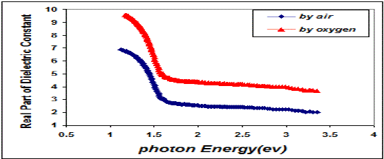 |
| Fig. 8 Variation real part of the dielectric constant & photon energy for CuO thin films |
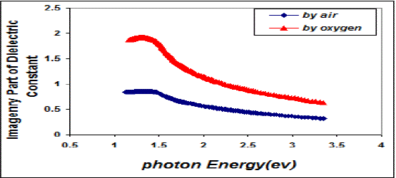 |
| Fig. 9 Variation imaginary part of the dielectric constant & photon energy for CuO thin films |
| This behavior may be due to the difference in growth behavior of CuO films during thermal oxidation processes. Figure (4) is a plot of absorption coefficient (α) as films as a function of photon energy for CuO thin films. It is observed that the absorption coefficient values increase when we used oxygen flow than air flow for thermal oxidation processes. This behavior may be due to the changes in the exits gas during thermal oxidation processes result in the change in stoichiometry of CuO and nanocrystallites size in these films .Thus, the observed change in the absorption coefficient. It is clear from this figure that all the films have high values of absorption coefficient (α > 104 cm-1) this means that the direct transition is possible occurs. This result is in agreement with refs [1] [3]. Figure (5) shows a plot of (α hν)2 versus photon energy (hν) to find the type of the optical transition for (CuO) films, which describes the allowed direct transition. The optical energy gap (Egopt) values were calculated from Tauc equation (2) by select the optimum linear part, which determined by the extrapolation of the portion at (α =0). The noticeable remark is that the Egopt decrease from (1.6 eV) to (1.45 eV) when we used oxygen flow than air flow for thermal oxidation processes. This behavior can be attributed to the decrease of the density of localize states in the Eg during thermal oxidation processes by oxygen which caused the energy gap seems small. The value of the optical energy gap is agree with ref. [1] which found it equal (1.6 eV) and [21]who reported a band gap range of (1.21-1.51) eV. The variation of the refractive index values (n) versus wavelengths in the range (300-1100) nm of (CuO) films is shown in Figure.(6) . We can notice from this figure that the refractive index values increase when we used oxygen flow than air flow for thermal oxidation processes, this behavior may be due to increase in packing density as a result the difference oxidation method. The high values of the refractive index of these films increases from (2.62 to 3.2) for the sample which oxidation with exist oxygen gas, the high refractive index possessed by these films makes it suitable for use as anti-reflection coatings. This is in good agreement with values reported in ref. [1] which found all samples have a peak refractive index of (2.7), and ref [3] who reported a refractive index range of (2.16-3.81.)Figure (7) is a plot of the extinction coefficient (K) as a function of photon energy for CuO thin films, we can notice from this figure that the extinction coefficient values increase when we used oxygen flow than air flow for thermal oxidation processes, this behavior of the extinction coefficient values similar for all the range of the wavelength spectrum to that of the absorption coefficients for the same reasons as we mentioned before. The variation of the real (ε1) and imaginary (ε2) parts of the dielectric constant values versus photon energy for CuO thin films are shown in figures (8),(9) respectively. From this figure we can deduce that both real part and imaginary part of the dielectric constant (ε2) increase when we used oxygen flow than air flow for thermal oxidation processes in all the range of the spectrum, this behavior may be due to the variation of (ε1) mainly depend on the value of the refractive index while the (ε2) value mainly depend on the extinction coefficient values which are related to the variation of absorption coefficient. |
CONCLUSION |
| In conclusion, we studied in detail the influence of exist air and oxygen during thermal oxidation processes for CuO thin films on the structural and optical properties. Throughout our research we shown that the structural analysis results of Cu thin films demonstrate that the single phase of Cu with high a crystalline structure with a preferred orientation (111). X-ray diffraction results confirm the formation of pure CuO phase in both methods of preparation. |
| The grain size decrease as we change the method of preparation from air to oxygen, and a strong absorption at wavelength range of (300-410) nm, which is make Copper Oxide films suitable for solar cell. All films prepared have high values of absorption coefficient (α > 104 cm-1). The absorbance values increases while the transmittance value decrease when we used oxygen flow for thermal oxidation processes .Copper Oxide films have high transmittance in the NIR region, which makes these films suitable for solar energy collection. The optical energy gap values decrease when we used oxygen flow for thermal oxidation processes. The values of all optical constant (absorption coefficient, refractive index, extinction coefficient, and dielectric constant) are increases when we used oxygen flow for thermaloxidation processes . |
References |
|