International Journal of Innovative Research in Science, Engineering and Technology
ISSN ONLINE(2319-8753)PRINT(2347-6710)
ISSN ONLINE(2319-8753)PRINT(2347-6710)
Zaheer Ahamed1, Ravishankar K.M2 , A.R.Anwar Khan3
|
| Related article at Pubmed, Scholar Google |
Visit for more related articles at International Journal of Innovative Research in Science, Engineering and Technology
The combination of two ceramic materials gives very good results. The same two ceramic materials when synthesized at nano level give extra-ordinary results. In this context, this research project uses alumina and silica as two ceramic materials. They are synthesized with the aid of electron beam lithography. PMMA is used as resist material instead of negative resists. This is because of the PMMA resist will give the desired results. It is spin coated with 6000 rpm in order to get the desired results. Then this is used in electron beam lithography which is a maskless lithography and which overcomes the limitations in mask lithography. After co-deposition of Al2O3 and SiO2 with the help of sputtering then finally characterization has taken place. In this characterization, Scanning electron microscope (SEM) images are taken and then finally atomic force microscope (AFM) images are taken in order to know the 3D images, adhesiveness, and surface roughness.
Keywords |
| ceramic materials, alumina, silica, sillimanite, kyanite, andalusite, mullite, electron beam lithography, scanning electron microscope and atomic force microscope. |
I. INTRODUCTION |
| Nanomaterials are stepping stone of nanoscience and nanotechnology. Nanostructure science and technology is a broad and interdisciplinary area of research and development activity that is growing rapidly worldwide since few years. It has the potential for revolutionizing the number of ways in which materials and products can be created. Nanoscale materials are defined as a set of substances where at least one dimension is less than approximately 100 nanometers. A nanometer is one millionth of a millimeter - approximately 100,000 times smaller than the diameter of a human hair. Nanomaterials are of interest because at this level they have unique optical, magnetic, electrical, and other properties emerge. These emerging properties have the potential for great impacts in electronics, medicine, and other fields. They can also be found in sunscreens, cosmetics, sporting goods, stain-resistant clothing, tires, electronics, as well as many other everyday items, and are used in medicine for purposes of diagnosis, imaging and drug delivery. |
| These nano materials can be synthesizes by two ways i.e top down and bottom down approach. In top down, materials are produces by chipping and carving out the excessive material like in the case of making the sculpture. Whereas the bottom up process, it involves building up the materials or structures atom by atom or molecule by molecule. Both have their own advantages and disadvantages. Depend upon the application one has to select the appropriate approach for the production of nano materials. The electron beam lithography is the one of the best top down approach for the synthesis of nano materials. EBL is well known for its maskless lithography for a better control over line width i.e less than 5 nm. Only one disadvantage of using this technique is it takes too much time for writing the pattern onto the resist material. After transferring the pattern onto the PMMA resist, the desired material can be synthesized with the help of sputtering (electron beam evaporation or thermal evaporation). Sputtering means ejecting material from a target and depositing it on a substrate such as a silicon wafer. The target is the source material. |
II. LITERATURE REVIEW |
| Alumina (Al2O3) |
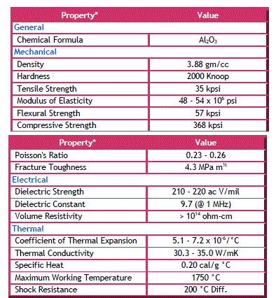
| Alum was known to the Sumerians, Egyptians, Greeks and Romans who used it for a wide variety of applications as an astringent (medicine for stopping flow of blood), as mordant for wool dye, as tan for skins, as an anti-inflammatory product, as a healing substance, as an anti-per spirant, as an anti-diarrhoeal product, for embalming and fireproofing of wood. Fused alumina (the substance produced after being melted and re-crystallized) is identical in chemical and physical properties with natural corundum. It is a very hard material and its hardness is exceeded only by diamond and a few synthetic substances such as carborundum, and silicon carbide. This property of alumina lends itself for use as an abrasive material. Another useful property of the material is its high melting point, i.e., above 2000°C (3632°F), which makes it useful as a refractory and as linings of special furnaces. (“Alumina” Britannica) The mechanical, chemical, and electrical properties of Alumina (99.7% purity) often used in the ceramic industry. |
| Silica (SiO2) |
| One of the most dangerous kinds of dust you can breathe is crystalline silica. Silica is in sand, rock, masonry, concrete, and some paints. (Quartz is silica.) You can be exposed to silica when you work with these materials in abrasive blasting, cutting/sawing, jack hammering, grinding, drilling, crushing, or dry sweeping – or during demolition of concrete or masonry structures. Silica occurs commonly in nature as sandstone, silica sand or quartzite. It is the starting material for the production of silicate glasses and ceramics. Silica is one of the most abundant oxide materials in the earth's crust. It can exist in an amorphous form (vitreous silica) or in a variety of crystalline forms. Often it will occur as a non-crystalline oxidation product on the surface of silicon or silicon compounds. The pure form of Silica is Quartz and the impure form is sand. Mainly it is used with aluminium in car manufacturing industries. Used in waterproofing treatments, moulding compounds and mould-release agents, mechanical seals, high temperature greases and waxes, caulking compounds and even in applications as diverse as breast implants and explosives. It is used to keep the metal conductors from fusing in order to prevent short-circuit so that the cables remain operational during a fire, which can be important for applications such as emergency lighting. Thin films of silica grown on silicon wafers via thermal oxidation methods can be quite beneficial in microelectronics, where they act as electric insulators with high chemical stability. In electrical applications, it can protect the silicon, store charge, block current, and even act as a controlled pathway to limit current flow. In microelectronics, it is used as thin layers of pure SiO2. The layers are amorphous and the density ranges from 2.0 - 2.3 gm/cm3. In its capacity as a refractory, it is useful in fibre form as a high-temperature thermal protection fabric. In cosmetics, it is useful for its light-diffusing properties and natural absorbency. Colloidal silica is used as a wine and juice fining agent. In pharmaceutical products, silica aids powder flow when tablets are formed. Finally, it is used as a thermal enhancement compound in ground source heat pump industry. |
III. EXPERIMENTAL PROCEDURE |
| Materials used |
| Alumina (Al2O3) is very hard material and its hardness is exceeded only by diamond and a few synthetic substances such as carborundum, and silicon carbide. This property of alumina lends itself for use as an abrasive material. Another useful property of the material is its high melting point, i.e., above 2000°C (3632°F), which makes it useful as a refractory and as linings of special furnaces. |
 |
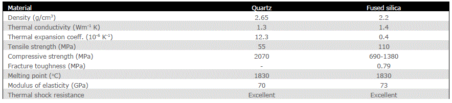 |
| The pure form of Silica (SiO2) is Quartz and the impure form is sand. Mainly it is used with aluminium in car manufacturing industries. Used in waterproofing treatments, moulding compounds and mould-release agents, mechanical seals, high temperature greases and waxes, caulking compounds and even in applications as diverse as breast implants and explosives. |
 |
IV. PROBLEM DEFINITION |
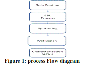
| Process flow |
| The first step in the first stage is sample preparation where SiN wafer is cleaned with Piranha solution. After cleaning of this substrate it is dipped into dil. HF. Then dehydration process will takes place with a prebake temperature of 150 0C for about 5 minutes. Then Spin the PMMA resist at 6000 rpm in order to get 200 nm thickness for 60 seconds. The spin off stage takes place for approximately 10 seconds after spin up. |
 |
| After obtaining 200 nm thickness of PMMA resist then it is used for soft bake at 95 0C for 45 seconds. |
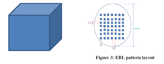 |
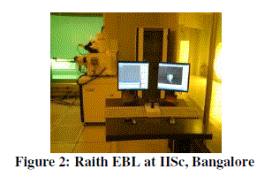
| In this experiment Raith EBL equipment (shown in above figure) is used to produce the desired pattern and the wafer along with PMMA deposition is kept in the sample loading unit of EBL. Raith uses NPGS (Nano pattern Generation System) software to design the layout of the pattern and the generated pattern is as shown in figure 3. Each cube consists of 50 nm x 50 nm x 50 nm. |
 |
| In this process, it is proposed to synthesis 50nm cubes of 7*7 matrix. The diameter of the wafer is 4 inch and whereas the thickness is 525 μm. The film of resist are exposed to line dose of 1-2 nC/cm and area dose of 200 mC/cm2 at 30 kV of energy beam depending on the pattern. Then finally allow the electrons from the electron gun from electron source towards PMMA resist in order to deposit the desired pattern which was designed. It took 7 hours of time to deposit the desired pattern. Then finally lift-off process is conducted on the specimen in order to remove the unwanted PMMA resist and to get the final desired pattern which will be ready for next process i.e, sputtering process. In this process the material to be deposited is taken for co-deposition and is kept in sample holder. Then allow high voltage current in order to evaporate from the sample holder and allow it to deposit on to the silicon nitride wafer i.e on to the holes as well as on the PMMA resist. Then allow it for solidification. |
 |
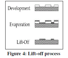
| The lift-off process is used in order to chip-off or remove the unwanted PMMA resist as well as to remove the unwanted deposited material with the help of sputtering process. The final specimen will look like as shown in the figure 4. This specimen is further is used for characterization for SEM and AFM. |
V. EXPERIMENTAL RESULTS |
 |
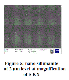
| The above figure shows the presence of nano sillimanite cubes of 50nm side at 100 μm level at a magnification of 250X. |
| The figure 5 shows the SEM image of nano sillimanite cubes. It is seen at 2 μm level at a magnification of 5 KX. From this it is clearly visible that the presence of nano sillimanite is available on silicon nitride wafer. The white dots indicate the co-deposition of alumina and silica materials. Whereas the remaining dark area indicates the silicon nitride wafer. |
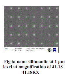
| In the above sem image, sillimanite material is seen at 1μm level with a magnification of 41.18 kx. From this image some of the cubes are not seen and this may be reason of contamination after synthesis which exists on the silicon nitride wafer |
| 2. AFM analysis |
| 3D image analysis |
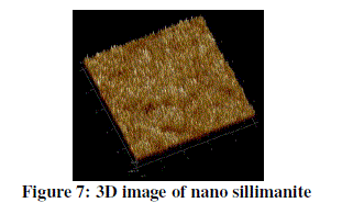 |
| The figure 7 shows the 3D image of sillimanite cube. The golden yellowish color shows the presence of silicon dioxide and whereas the white color indicates the presence of aluminium dioxide. The valleys present in the image indicate the presence of any voids. |
| 3. Surface roughness |
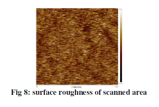 |
| The above figure shows the surface roughness values at various locations of the scanned area. The area of scanning is 25.5 μm2. Mostly there are two colors in the AFM image, one is dark brown and light brown. The dark brown has zero value for surface roughness and whereas light brown indicates that it has an average roughness value i.e 1.21 nm. The maximum surface roughness on the scanned area is 12.4 nm and this is shown in white color in the above figure. The presence of two ceramic materials at nano level has almost negligible roughness value. |
| 4. Adhesive force |
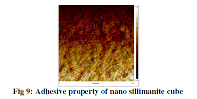 |
| The above figure shows the adhesive property and from the figure it is very clear that this image is taken from 0 – 5 μm range. There are various colours on the plot. The whitish colour indicates that the material have more adhesive force (1.1 μN) towards the tip of the cantilever beam. That means there is a frictional force behind this phenomenon. Whereas the dark brown colour indicates that there a less adhesive force (80 nN) exists when we move from center of the material towards the edge of the material. And this value again very less when we move towards the edges of the specimen (i.e. 58.4 nN). |
VI. CONCLUSION |
| It seen from the SEM images that the distribution of the nano sillimanite tiles of 50 nm is uniform throughout the scanned surface area. It is seen from the image that 50nm cubes are clearly visible. The white spotted areas indicate that the presence of nano sillimanite tiles whereas the dark area indicate silicon nitride wafer. From the AFM images it is seen almost a flat surface except with some valleys. It has very good adhesiveness property with the tip of the cantilever beam of the atomic force microscope. The combination and presence of two ceramic materials will give almost zero surface roughness i.e 1.21 nm which is almost negligible. The maximum surface roughness at the peaks and valleys is 12.4 nm. |
References |
|