International Journal of Innovative Research in Science, Engineering and Technology
ISSN ONLINE(2319-8753)PRINT(2347-6710)
ISSN ONLINE(2319-8753)PRINT(2347-6710)
Nalini.N, Ms.M.SheelaSankari
|
| Related article at Pubmed, Scholar Google |
Visit for more related articles at International Journal of Innovative Research in Science, Engineering and Technology
This paper describes the non-isolated high step-up DC-DC converter using Zero Voltage Switching (ZVS) Bi-directional Integration Technique (BIT). The DC-DC converter which integrates PV and battery power for high step up applications are proposed. Coupled inductors are used to attain the high step up voltage gain and also used to reduce the voltage stress of input side switches. The operation need not to be changed when the transition between charging and discharging occurs. It is also capable of operating simultaneously in tracking the maximum power from the sun and generates the output. This implies the usage of PV panel most of the time.
INTRODUCTION |
| The general approach to the application is a classical boost converter which is simple in its structure and gives continuous input current and also provides the clamped switch voltage stress to the output voltage. The integrated multiport converters for interfacing several power sources and energy storage elements are widely used in the recent years.Instead of using separate power electronic converters for every energy sources, multiport converters have few advantages such as usage of fewer amounts of components, lower cost, compact in size and dynamic performance is better. In several conditions atleast one storage device should be used. |
| A coupled inductor employed in a boost converter is a suitable for step-up technique for its compact structure. It is also possible to achieve a high efficiency and protect switch from the high peak voltage and auxiliary circuit is required to suppress the switch voltage stress and it is also capable ofachieving a high soft switching performance. Alternative way of easy approach for a high step up ratio is the current fed type converters with the usage of a transformer. The transformer leakage inductance cause the voltage spikes across the switches so the snubber circuit is needed which results in the additional losses. |
| In view of the clamp capacitors are connected to the input side so that it has no function of extending the step-up ratio. On focusing the step-up ratio extension with the concept of stacked output capacitors, the high step up boost flyback converter is proposed and improved with the secondary voltage-double rectifier. Instead their high step-up capability, the switch suffers from the hard and severe switching losses. |
| Various types of topologies are proposed due to the advantages of the multiport converters. The combination techniques for the multiport converter include sharing of switches, capacitors, inductors or magnetic cores. It is important to select a proper topology by considering several aspects which includes cost, reliability and flexibility depending on its applications. An application of hybrid energy supply using renewable energy resources and storage devices is shown in Fig. 1. |
| The DC microgrid enabled by the solid-state transformer (SST) in the Future Renewable Electric Energy Delivery and Management System (FREEDM System) which integrates various distributed renewable energy resources (DESDs). For certain instance, if solar power is selected as the renewable energy source and battery as the storage device. The battery can either supply load with solar energy at the same time or it also stores the excess power from the solar panels for backup purpose.Many multiport converter topologies are implemented in the literature and it can be divided into two categories.One is nonisolated type- the non-isolated convertersare usually derived from the typical buck, boost, or buck– boosttopologies and are more compact in size. The other is isolated type -the isolated converters using bridge topologiesand multi-winding transformers to match wide input voltageranges. |
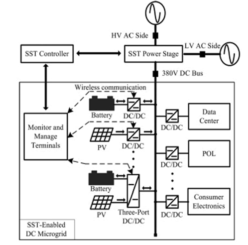 |
| Fig. 1Part of the FREEDM system diagram showing an SST-enabled DC microgrid. |
| A topology based on buck configuration is used in airplanes and space-craft front-end system. The battery port in this converteris unidirectional, so the battery cannot be charged from the photovoltaic (PV) port. A multi-input buck–boost type converter is proposed to interface manyrenewable energy sources but there is no bidirectional port tointerface the battery. A two-input converter for a hybrid fuel cell(FC)/battery power system is implemented with zero voltageswitching (ZVS) feature. Although the efficiency is improved,this converter could not provide a high voltage conversion ratio and bidirectional functionality. A multiple-input converterbased on a boost topology is presented in that has lower input current ripple and therefore is suitable for the large currentapplications such as hybrid vehicles. |
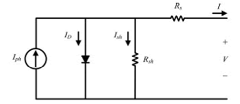
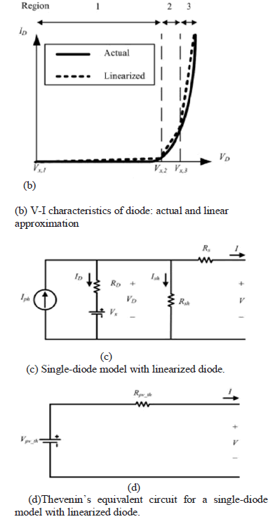
| Thevinin’s theorem is not valid for the non-linear model, but that non-linear model is represented by the linear with non-constant parameters. For example, the piecewise linearization is used to linearize the diode. The parameters in Fig. 2(a) can be estimated using the manufacturer’s datasheet [39]. As shown in Fig. 2(b), the actual diode characteristic has been divided into three regions and the characteristic in each region is approximated as a straight line. Each line can be further represented by a set of voltage source Vx,n and resistanceRD ,n (n = 1,2,3). The approximation of piecewise linearizationwould be more accurate as the number of regions increased. Atthe boundary points of regions, the values of linearized characteristic are exactly the same as actual characteristic. Therefore,the maximum power point of the PV generator is chosen as one of the boundary points such that the operation at this pointhas no approximation error. The single-diode model of the PVgenerator with linearized diode is shown in Fig. 2(c), where thediode is approximated by the voltage source Vx , and resistanceRD . The values of Vx and RD are dependent on the operationregion of the PV generator. The Thevenin’s equivalent model of Fig. 2(c) is shown in Fig. 2(d). |
OPERATION OF THE TOPOLOGICAL MODES |
| Before performing the analysis, some assumptions should bemade: |
| 1) The switches are assumed to be ideal; |
| 2) The magnetizing inductors are large enough so that the current flowingthrough the inductors are constant; |
| 3) the capacitors are largeenough so that the voltages across the capacitors are constant. |
 |
| Fig: 2 .Thevinin’s equivalent circuit derived from the single-diode model. (a)Single-diode model of a PV generato |
 |
Zero Voltage Boost Integration Technique (ZVSBIT): |
| Fig. 3 shows the conceptual diagram of ZVS BIT. A seriesoutput module is connected to a bidirectional boost converteras a PISO configuration. This series output module can be anyisolated current-fed type converter. Also, it can adopt any kindof secondary rectifiers such as the full-bridge, center-tapped, voltagedoublers, and so on. |
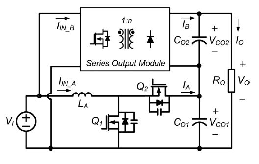 |
| Fig. 3 Conceptual diagram of ZVS-BIT |
3.1).High Device Utilization: |
| To increase the device utilization and simplify the circuit, thecommon parts integration between a series output module and abidirectional boost converter is recommended. A flyback converter can be integrated easily since the boost inductor LA and switch Q1 in Fig. 1 become the flyback converter counterparts. |
| High Step-up Capability: |
| Due to the stacked output capacitors, each output capacitorvoltage is added and the overall output voltage can be extendedas |
| VO = VC O 1 + V C O 2 . (1) |
| That is, the output voltage of the converters employing the proposed ZVS BIT is a sum of the output voltages of the boostconverter and the series output module, which is suitable forhigh step-up applications |
Power and Thermal Stress Distribution |
| By imposing the node equations on the output capacitor CO 2, the steady-state output current equation can be derived as |
| IO = IA (t) = IB (t) (2) |
| Where Io denotes the average value of I. Equation (2) impliesthe power distribution between the bidirectional boost converterand the series output module isproportional to each outputvoltage. Therefore, the thermal stress can be decentralized. |
| Since the same average current flows through each outputcapacitor, the current distribution at the primary side is alsopredictable and can be expressed as follows: That is, the current distribution ratio at the powering phase onlydepends on the transformer turns ratio n, which decides the slopeof the primary current Ipri (t) while Q1 is turned off. The powering current distribution depictedby the diagonal-lined and vertical-lined areas satisfies (2) and(3). |
| Switch Voltage Stress Clamping: |
| The switch voltage stresses VQ 1 and VQ 2 can be clampedto the partial output voltage VC O 1. Thus, additional protectioncircuit for the high voltage spike caused by a leakage inductorLlkg is not required. |
| Soft Switching Capability |
| The proposed ZVS BIT seems to be an active-clamp network,which is not connected to the input side but the output side.The previous works regarding the activeclamp circuit concentrate on the soft switching capability and switch voltage stressclamping [10]–[12], [17]–[21]. However, the proposed ZVS BITprovides these abilities as well as the step-up ratio extension because of the series output connection of the clamp capacitor. |
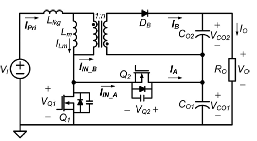 |
| Fig. 4 ZVS flyback boost converter |
| The soft switching characteristics are similar to the active-clamp circuit. A main switch Q1 has a loaddependent ZVScondition relying on the value of the leakage inductor Llkg ,whereas an auxiliary switch Q2 has a wide ZVS load rangeresulting from a large boost inductor Lm . Thus, all switches canbe turned on under ZVS condition if the energy stored in Llkg is sufficient. |
| However, since ZVS condition of Q1 is loaddependent andlost at a light load due to the insufficient leakage energy, theefficiency degradation caused by switching loss is inevitable. |
COMPARISON OF DC-DC BOOST CONVERTERS: |
| In order to satisfy the stringent requirements with performance in renewable energy grid-connected power applications, many researchers concentrateon how to realize high voltage gain step-up, low cost andhigh efficiency single-stage converters [12]. The brief comparison of available single-stage transformer less converters will be presented below. They provide the voltage gain up to 20using coupled inductors or switched capacitor technique. Usually the efficiencies of high voltage gain step-up convertersare at the levels over 90% at sub kilowatt or single kilowatt powers. To increase the overall efficiency of converter softswitching technique [8] as well as active clamped circuit [12]introduction may be considered. Boost converter. The single phase single switch boostconverter is a basic step-up topology [32]. The voltage gain theoretically is infinite when duty cycle reaches 1.But switch turn on period becomes long as the duty cycle (D)increases causing conduction losses to increase. |
| The powerrating of single switch boost converter is limited to switchrating. In order to obtain higher gain several boost converterscan be cascaded at the expense of efficiency decrease. Inter-leaved parallel topology is the solution to increase the powerand reduce input current ripple allowing lower power rated switches to be used. |
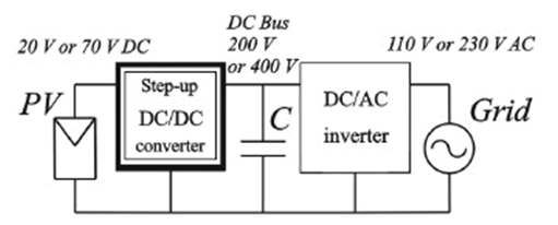 |
| Fig. 5 PV converter with integrated DC/DC converter. |
| Software description |
| MATLABis a high-level language and interactive environment for numerical computation, visualization, and programming. Using MATLAB, you can analyze data, develop algorithms, and create models and applications. The language, tools, and built-in math functions enable you to explore multiple approaches and reach a solution faster than with spreadsheets or traditional programming languages, such as C/C++ or Java |
| MATLAB is a program that was originally designed to simplify the implementation of numerical linear algebra routines. It has since grown into something much bigger, and it is used to implement numerical algorithms for a wide range of applications. The basic language used is very similar to standard linear algebra notation, but there are a few extensions that will likely cause you some problems at first. |
| The goal of the tutorials here is to provide a simple overview and introduction to mat lab. The tutorials are broken up into some of the basic topics. The first includes a few examples of how Mat lab makes it easy to create and manipulate vectors. The tutorials move from the simple examples and lead to more complicated examples. |
Results and Discussions |
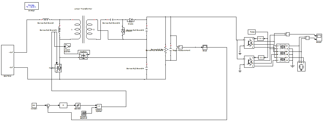 |
Methods Entire simulation diagram ofDC-DC converter with grid connected system. |
| Figure 6 shows the experimental set-up of the DCDc converter which is feed the input by solar panel and the output of the converter is inverted and connected to the grid system or residential loads. PI controller is used for the performance of the closed loop operation. Three phase inverter is used for the inversion of output voltage from boost converter with the implementation of ZVS BIT technique. The boosting value is high in the ratio of 1:10 in the output by the connection of linear transformer which reduces the high switching losses. |
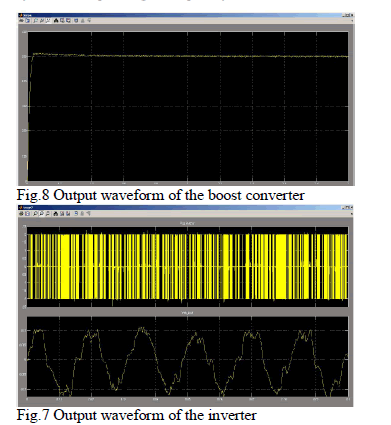 |
| The boost converter gives the high range of output when compared to the input voltage from the solar panel and dc source. The inverter output having some ripples because of the electronic components in the circuit. |
Conclusion and future work: |
| Non-isolated high step-up DC-DC converters using ZVS BIT is presented in this paper. The proposed ZVS BIT integrates the common parts between a bidirectional boost converter and a series output module. The simple but effective ZVS BIT gives many desirable features for high efficiency and high step-up applications. With the concept of ZVS BIT, a ZVS flyback-boost converter with VDR is derived and investigated in detail as an example. All theseworks are verified experimentally with a digitally controlledprototype converter. Although the efficiency improvement byZVS BIT is prominent in a ZVS load range, it does not appearat light load condition. Therefore, the proposed ZVS BIT control can be a promising solution for high step-up applications.In the proposed topology, two coupled inductors are employed as voltage gain extension cells for high voltage output applications. Two sets of buck–boost type active-clamp circuits are used to recycle the energy stored in the leakage inductors and improve the efficiency. The proposed switching strategy only needs to control two duty ratios in different operation modes. A high step-up three-port DC–DC converter for stand-alone power systems is proposed to integrate solar and battery power.In light-load condition, once the charging voltage is higher than the present level, the operation mode will be changed rapidly to protect the battery from overcharging. The highest converter efficiency is measured as 90.1% at 110W. The control method of the battery port could be modified for the grid-connected applications. |
References |
|