International Journal of Innovative Research in Science, Engineering and Technology
ISSN ONLINE(2319-8753)PRINT(2347-6710)
ISSN ONLINE(2319-8753)PRINT(2347-6710)
Jasirah.K.B 1, Atrhira.P.C 2
|
Visit for more related articles at International Journal of Innovative Research in Science, Engineering and Technology
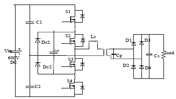
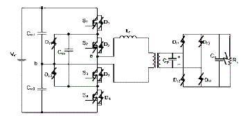
Fault detection and protection is an important design aspect for any power converter, especially in high power high-voltage applications, where cost of failure can be high. The three-level dc-dc converter and its varied derivatives are attractive topologies in high-voltage highpower converter applications. The protection method can not only prevent the system failure against unbalanced voltage stresses on the switches, but also provide a remedy for the system as faults occur and save the remaining components. The three-level converter is subject to voltage unbalance in certain abnormal conditions, which can result in switch overvoltage and system failure. The reasons for the unbalanced voltage stresses are fully investigated and categorized. The solutions to each abnormal condition are introduced. In addition to the voltage un balance, the threelevel converters can be protected against multiple faults by the proposed protection method through monitoring the flying capacitor voltage. The protection circuit is simple and can be easily implemented, while it can effectively protect the threelevel converters and its derivatives, which has been verified by the experiment with a three-level parallel resonant converter.
Keywords |
| Flying capacitor, protection, three-level dc-dc converter, voltage unbalance. |
INTRODUCTION |
| Reliability is always a concern for power converters. Faults can occur even in carefully designed circuits. Fault detection and protection is an important design aspect for power converters, especially in high-power high-voltage applications, where cost of failure can be high and the consequence of failure can be serious.For dc–dc high-voltage high-power converter applications, the three-level dc–dc converter and its varied derivatives are attractive topology choices.The main advantage of three-level dc–dc converters is that the main switches only withstand half of the input dc-link voltage, so lower voltage rating devices with better performance can be used. On the other hand, three-level converters need to have balanced dc voltages Vcin1 and Vcin2 and two clamping diodes to ensure proper operation and equal voltage sharing .The flying capacitor is initially introduced by Francisco for the phase shift operation..The flying capacitor can help to decouple the switching transition of the outer two switches (S1and S4) and the inner two switches (S2 and S3). When one of the outer switches turns OFF, its parallel capacitor is charged, and meanwhile the parallel capacitor of the other outer switches discharged through the flying capacitor so that zero voltage switching (ZVS) can be achieved. The two capacitors in parallel with the inner two switches do not participate in this switching transition and vice versa. Furthermore, with phase shift pulse width modulation (PWM) control, the flying capacitor is essentially connected in parallel to the input capacitors during the freewheeling stage of the converter alternatively. Therefore, the flying capacitor can alleviate the voltage imbalance of the input capacitors with phase shift PWM operation .In addition, the flying capacitor also works as a snubber capacitor for the two inner switches. Under normal operating conditions, Vcss should have a nominal voltage equal to Vin/2. An abnormal Vcss may indicate an abnormal circuit condition or fault, which can be used as the basis for fault detections. |
 |
| First, with the traditional operation schemes, the reasons thatcause the abnormal voltage stresses are thoroughly analyzed and categorized, as well as the solutions according to the different reasons. In essence, these issues can be fixed or avoided in a normal converter design and operation, as is stopped by protection circuit. Then the possible faults of the three-level parallel resonant converter(PRC) are systemically analyzed and summarized with the help of simulation in section III. In Section IV, a protection circuit with fast response time is presented, along with the flying capacitor design and the circuit design criteria. Finally, SectionV provides experimental results to verify the analysis and the protection functions. |
OPERATION PRINCIPLE AND SOLUTIONS TO UNBALANCED VOLTAGE STRESS |
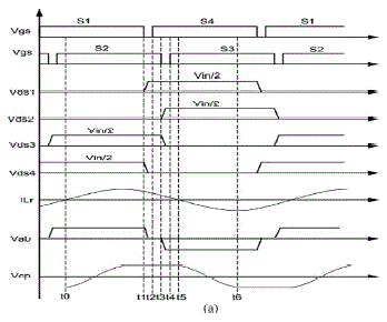
| The typical waveforms for three-level parallel resonant converter with phase-shift (PS) and PWM operation modes. Since both operation modes have to guarantee that the outer switch (S1 or S4) should be turned OFF no later than the inner switch (S2 or S3) in the same leg for ZVS achievement. The problem of voltage unbalance across the switches in the same leg at two specific conditions, with open voltage loop control and at light load. However, Vcss could also be changed under other various conditions, such as zero-current-switching(ZCS)/non-zerovoltage switching(ZVS)operation, high voltage ripple on input capacitors, unbalanced switching timing, etc. In essence, these can be fixed when the problem is stopped by protection and located. The solutions to the issues are introduced. A thorough analysis on abnormal conditions is necessary for designers to understand the converter operation and know the limits so that a protection can be designed to tolerate to normal operation without losing sensitivity.These abnormal conditions can be classified into three main categories, as enumerated in the following. |
 |
| A. Abnormal Input Capacitor Voltages Due to Input Voltage The voltage across the two input capacitors (Cin1 and Cin2) are needed to split the input voltage equivalently, and the neutral point, has half of the input voltage (Vin/2). So the neutral point voltage and Vcss are fundamentally determinedly the input voltage. If the input voltage varies beyond the allowed range, obviously, the over/under input voltage lockout can be triggered by monitoring the Vcss. |
 |
| B.Abnormal Input Capacitor Voltages Due to Unbalanced |
| Another main abnormal performance of input capacitor voltages is unbalanced voltage. When the voltage across Cin1 is higher than Vin/2, the flying capacitor will be charged through down clamping diode Dc2.If the Cin2 voltage is higher than Vin/2, the flying capacitor will be charged through clamping diode Dc1.More explicitly, the flying capacitor will be paralleled with the input capacitor which has high voltage stress. It should be noted that this is also why the flying capacitor helps to alleviate the voltage unbalance of the input capacitors .No matter which input capacitor has higher voltage, or, in other words, no matter the neutral point has higher or lower voltage than Vin/2, the flying capacitor voltage will be charged to the peak voltage of the input capacitor with a higher voltage. So unequal capacitances of input capacitors, unbalanced duty cycles or mismatched switching timings, etc., belong to this case, which contributes the unbalanced input capacitor voltages and then the abnormal flying capacitor voltage. When the problem is caused by these issues, it can be easily solved in circuit. Normally these tiny unbalancedcapacitances and duty cycles can be tolerated without serious consequence. In addition, the unbalanced duty cycles can be alleviated by the flying capacitor in the phaseshift operation. A control circuit to balance the unsymmetrical duty cycles by monitoring voltage across the flying capacitor for the nonphaseleg structure converter, such as buck, boost .It also can be adjusted for the circuit with the phase leg structure when the unbalanced duty cycle is an issue. Moreover, even if the voltages across the input capacitors are balanced, the Vcss still can be influenced by the voltage ripple on the input capacitor. converter, loss will be high due to the input diode bridge. |
| C.Losing Discharging Path EvenWith Normal Input capacitor voltage |
| Even if the neutral point voltage is normal, the unbalanced voltage stresses still can happen in some conditions. In a normal operation, the flying capacitor can be charged through the upper clamping diode (Dc1) or S1. Or it can be charged through bottom clamping diode (Dc2) and S4 due to the symmetrical structure. The only possible discharging path for flying capacitor is through S2 or S3. If the flying capacitor can be charged through S2 or S3 instead of discharging in some conditions, the flying capacitor voltage will definitely increase because it has no way to decrease. With the conventional ZVS control (S1 is turned OFF beforeS2, and S4 is turned OFF before S3), the commutation of the phase shift provides a discharge loop for flying capacitor when ZVS operation is desired. However, when the converter loses ZVS, such as at light load; or the switching timing is wrong, such as when S2 is switched OFF before S1 or S3 is switched OFF before S4 the flying capacitor will be charged instead of being discharged. The Vcss could increase to approximate the input voltage due to no discharging loop. The current in the inductor has changed its direction when S1 is turned OFF. The upper side of the flying capacitor is connected with the input voltage through the body diode of S1. And the bottom side of the flying capacitor is connected with the ground when S4 is turned ON after S1 is OFF. In this case, the flying capacitor will be charged to full input voltage instead of discharging. Due to the symmetrical structure, this case can happen when S1 is turned ON after S3 is OFF. At light load, if the converter loses the ZVS operation for the lagging switch, or even worse, loses ZVS for both leading switch and lagging switch, the mechanisms the same as the ZCS condition. In order to solve this issue ,ZVS has to be guaranteed in the three-level converter design for all of its operation conditions, from heavy load to light load.WhenS2 is turned OFF before S1, the upper side of the flying capacitor is connected to the input voltage through S1 and the lower side of the flying capacitor is connected to the ground through the body diode of S4. Thus, the flying capacitor suffers the full input voltage. In order to solve this problem, the switch sequence has to be assured. Minimal phase-shift is desired to reduce the duty cycle loss when the regulation is through varying frequency instead of the duty cycle. If the abnormally high Vcssis owing to slightly too small phase shift, enlarging the phase shift or paralleling external capacitors in the inner switches is an effective way to solve this problem. However, it should be noted that the increased capacitance on the inner switch will worsen its ZVS condition. |
 |
MULTIPLE FAULTS IN THE THREE-LEVEL CONVERTER |
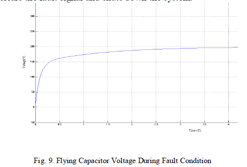
| The behavior of the flying capacitor voltage Vcss under various fault conditions in the three-level parallel resonant converter .The most common faults associated with the active devices and load, including open- or short circuit of main switches S1 and S2,clamping diodes Dc1, anti parallel diodes D1 and D2, rectifier diode Dr1 and load. The anti parallel diodes D1 and D2 short-circuit will be the same as the corresponding main switch short-circuit, only the open circuit of these anti parallel diodes need to be included. When the main switch is MOSFET, its body diode is commonly used as anti parallel diode instead of the external diode. It should be noted that the main switch cannot work properly if its body diode fails. Due to the symmetrical structure, the results will be the same as the counterpart failures occur. To some extent, the fault condition is the worst case of these abnormal conditions. For example, when S2 fails to open circuit, it is like avoiding the rule that S2 should be turned OFF no earlier than S1. |
 |
| A. Outer Switch Open Circuit |
| If outer switch (e.g., S1) has an open circuit, the loop is still complete for inductive load current so that the energy in When the switchthe bottom input capacitor, Cin2, is continuously transferred to load when S3 and S4 are ON. However, when S3 and S4 are OFF and S2 turns ON, the upper input capacitor (Cin1) will be isolated because the upper clamping diode (Dc1) will provide a short-circuit loop for the inductor current. But the energy in the bottom input capacitor, Cin2, will gradually discharge to 0, as does Vcss. The transformer will be saturated soon due to negative biased dc voltage stress. |
| B. Outer Switch Short Circuit |
| If S1 has a short circuit, the flying capacitor will be directly connected with input power source when S3 and S4 are ON. Vcss is equal to full input voltage, as does S2. But the neutralpoint voltage would not be influenced by this fault. |
| C. Inner Switch Open Circuit |
| If S2 has an open-circuit fault, Vcss also increases to full input voltage soon. The mechanism is the same as the outer switch short-circuit case, i.e., both violate the rule that S1 has to turn OFF before S2 turns OFF. When S2 fails to open circuit, t means that S2 always turns OFF before S1 . |
| D.Outer Switch Short Circuit |
| If S1 has a short circuit, the flying capacitor will be directly connected with input power source when S3 and S4 are ON.Vcss is equal to full input voltage, as does S2. But the neutral point voltage would If S2 has a short circuit, when S3 and S4 turn ON, the flying capacitor will be shorted through S2, and S3 and the bottom input capacitor Cin2 will be shorted through the upper clamping diode, S2, S3, and S4.Meanwhile, S1 has to withstand full input voltage when it is open. When S3 and S4turn OFF, the fault does not effect the converter operation as usual and the flying capacitor and Cin2 will be charged back to half of the input voltage. Hence, the Vcss and neutral point voltage are pulses from zero to half of the input voltage with the same frequency as switching frequency. The transformer will be saturated soon due to the positive biased voltage stress. |
| E. Outer Switch Body Diode Open Circuit |
| If the switch S1’s body diode D1 fails due to open circuit, this fault does not have any effect on the converter operation. As when S4 turns OFF and S3 is still ON, the inductor current will go through the bottom clamping diode back to the resonant tank instead of D1 after the S4’s switch capacitor is charged to half of the input voltage and S1’s switching is discharged to 0. Even if it is good, the D1 will never be conducted or involved in any commutation. The system is never affected by this fault. Certainly, this fault is undetectable by Vcss. |
| F. Inner Switch Body Diode Open Circuit |
| If the switch S2’s body diode D2 fails due to open circuit, the converter can work when the S1 and S2 are ON. When theS3 turns OFF after S4 turns OFF, the inductor current starts to charge the S3 switch capacitor and discharge the S2’s switch capacitor. But the inductor current has no way to go after theS3’s switch capacitor is charged to half of the input voltage andS2’s switch capacitor is discharged to 0 due to the open circuit of D2.Therefore, S3 will suffer high voltage spike in this fault case. But the Vcss keeps the normal value. This fault cannot be detected unless the noise caused by high voltage spike triggers the protection. It is possible in practical application due to the high abnormal noise when ZVS is lost. |
| G. Clamping Diode Open Circuit |
| If the clamping diode Dc1 fails due to open circuit, the converter works normally if the converter is ideal. But the converter will practically lose the advantages of the threelevel structure without the clamping diode. As long as the switch’s voltage stresses are unbalanced, this fault will be detected by Vcss. |
| H. Clamping Diode Short Circuit |
| If the clamping diode Dc1 fails due to short circuit, the neutral point voltage will be connected with the positive polarity of the input voltage and charged to full input voltage when S1 is ON,so does flying capacitor. In this case, S1 suffers huge current when it is ON, or then S2 suffers over-voltage when it is OFF. |
| I. Rectifier Diode Open circuit |
| If the rectifier diode Dr1 fails due to open circuit, no more energy will be transferred to the load when the resonant capacitor voltage is positive. But the converter keeps transferring the energy to the load when the resonant capacitor is negative. This unbalanced energy transfer will result in a positive dc biased voltage stress to the transformer. The neutral point voltage will decrease to 0 while the Vcss increases to the full input voltage. It should be noted that the neutral point voltage will increase if the rectifier diode in opposite bridge is open circuit while the Vcss still increases. Either one could fail before the neutral point voltage and Vcss reach the input voltage. Meanwhile, the transformer suffers a negative dc bias voltage. |
| J. Rectifier Diode Short Circuit |
| If the rectifier diode Dr1 fails due to short circuit, the resonant capacitor will be shorted when the polarity of the resonant capacitor voltage is negative. More energy can be transferred to the transformer secondary side when S3 and S4 are ON. It follows that the neutral point voltage decreases and flying capacitor voltage increases. Same as Dr1 open-circuit fault case, the neutral point voltage will increase if the rectifier diode in opposite bridge is shorted while the Vcss still increases. |
| K. Load Open Circuit |
| If load open circuit happens, the output voltage will increase significantly due to the PRC inherent boost property. But the converter will operate normally except for high current when the switching frequency is higher than resonant frequency. Otherwise, the converter will lose ZVS operation and the fault will be detected by the increased Vcss. |
| L. Load Short Circuit |
| If load short circuit happens, the converter still keeps the ZVS mode due to the PRC property. Theoretically it cannot be detected by Vcss. But the turn-OFF current which depends on the switching frequency will increase due to the triangle current waveform. High voltage spike due to high turn-OFF current still may practically trigger the protection with Vcss detection. The response of Vcss to load open circuit and load short-circuit may vary in other three-level topologies because the inherent properties of PRC is dominated in these faults. Of all the possible contingencies, the protection against shootthrough is the trickiest one, and is very dependent on the parasitic inductance. In an ideal case, the voltages of the input capacitors and flying capacitors are equal to half of the input voltage without any parasitic inductance even during a shoot through fault. However, since the input wire inductance of the power supply (Lin ) shown in Fig. 14 is usually very large or at least relatively larger than the parasitic inductance after the input capacitor as well as the relatively larger input capacitance, the Vcss will be dropped sharply as shootthrough happens. |
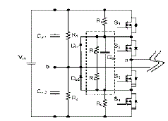
DESIGN OF PROPOSED PROTECTION CIRCUIT |
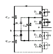
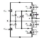
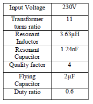
| For three-level structures, balance resistors are needed for the capacitors’ voltage balance the connection of balance resistors. R1 is equal to R2 , and R3 is equal to R6. In order to have half the input voltage, the sum of R4 and R5 is equal to the sum of R3 and R6 . For a protection circuit, R4 andR5 , with appropriate resistance, can be used as a voltage divider for the sensor of Vcss. For 600V input voltage, 1W 100 kΩresistors with 1% tolerance are chosen for R1 , R2 , R3 and R6 .R4 is 198 kΩand R5 is 2 kΩas a one hundredth voltage divider. The sensed voltage is processed by a window detector with an isolated auxiliary power supply. The window detector output is transferred to the system controller through a high-speed optocoupler. |
 |
| A. Flying Capacitor Design |
| Though the flying capacitor design is not directly related with the protection circuit design, the proposed protection method has to be based on the flying capacitor. In the conventional three level converter with phase-shift control, the functions of the flying capacitor as decoupling the switching transitions of S1 and S4, S2 and S3,balancing the unbalanced voltages between the two input capacitors, acting as a snubber capacitor for inner switches, S2 andS3. The decoupling effect is dependent upon on the ratio of capacitance |
 |
| where Vsw is the minimum left voltage of any one of switches when its gate signal is becoming high during switching transition.ZVS is achieved when Vsw is near 0. Css is the capacitance of flying capacitor. Csw is the sum of the capacitance of the switch capacitor and any external paralleled capacitor. For better decoupling and voltage clamping effect, the capacitance of the flying capacitor should be no less than the calculated number. Even if a phase shift control scheme is not employed and the flying capacitor is not necessary, the flying capacitor can still be added as a snubber capacitor and work for the proposed protection circuit. |
| B. Design Criteria |
| The Vcss is determined by the input voltage in steady-state operation. As the converter is running, the Vcss is mainly influenced by the voltage ripple of the input capacitors. Due to the clamping diode, the flying capacitor can be charged to the maximum voltage of the input capacitors, while the normal minimum Vcss is equal to the half of the low-line input voltage. |
| The duty ratio is given by |
 |
 |
 |
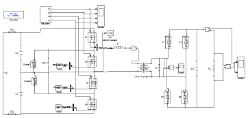
SIMULATION RESULTS |
| The transformer winding over-voltage breakdown results in secondary winding short circuit. The resonant capacitor is discharged to 0 suddenly, which is similar to the case of short circuit of one of rectifier diodes. The voltage stress of the inner switch, S3, immediately increases and is higher than the voltage stress of the outer switchingS4. The flying capacitor voltage is also abnormally increased. Therefore, the proposed protection is triggered and successfully protects the converter against the system failure. As the transformer is broken down, the resonant capacitor voltage is discharged to 0. Thus, the resonant inductor current waveform in becomes triangle waveform when the fault happens. In order to verify the analysis and the feasibility of the proposed protection, the scaled-down experiment is operated with 1/10ththe input voltage and the same prototype. |
 |
| The five selected faults respectively: S1short circuit, S1 open circuit, S2 short circuit, S2 open circuit, and shoot-through. The fault conditions are generated by a timer and a fault signal. The converter enters the steady state before the end of timer. At the end of timer, a fault signal, low level pulse, is added into one of gate signals with a logic AND gate to simulate an open-circuit failure. If the fault signal is a highlevel pulse, a short-circuit failure can be simulated when it is added into one of the gate signals through a logic OR gate. If the faultsignal is added into all of the gate signals, shootthrough will happen. When the protection circuit is triggered, a shut-down signal (V shutdown) will be generated, which clears the fault signal and shuts down the system. |
 |
| As S1 fails short circuit, the voltage across inner switch S2 immediately increases to full input voltage, as well as the flying capacitor voltage. The first two cycles correspond to normal operation. The protection circuit is triggered in less than 1 μs, which is indicated by the shutdownsignal.As S1 fails open circuit, the flying capacitor voltage gradually decreases, triggering the protection circuit. The fault had happened before the waveforms were captured. Compared with 30V of Vcss and drain to source voltage of S2(Vds2) at normal operation, the Vcss and Vds2 are about 20V, which triggers the low-level limit of protection. The notch of the drain to source voltage of S1 (Vds1) waveform is due to the S1’s body diode conduction. The clamping diodeDc1 has to withstand high conduction current when S2 turnsON.The S2 short-circuit case. The fault signal comes in the middle of the S2 OFF time while both bottom two switches(S3 and S4) are ON. The Vds1 quickly increases to full input voltage while the Vcss is discharged to zero and triggers the protection. The S2 open-circuit case. The fault signal comes before S2 and S1 are turned OFF. The Vcss starts to increase after the S2 fails to open circuit. Fortunately, soon it is time for the upper leg to turn OFF. Vcss keeps flat when S1 turns OFF the initial period when S1 turns ON again. When the inductor current changes the direction, the Vcss continues to increase, and then triggers the protection circuit. |
CONCLUSION |
| The proposed protection scheme based on flying capacitor voltage detection .The reasons for the unbalanced voltage stress is categorized. Solutions to each unbalanced voltage stress are introduced. The possible faults are thoroughly analyzed .The proposed protection method can effectively avoid the device failure caused by unbalanced voltage stresses on switches in the three-level structure, and will protect the system even if a failure occurs. Remedies can be taken to prevent the consequent damages of the faults when the new protection method is employed. A detection circuit is proposed, and its design is addressed as well as flying capacitor selection. The theoretical analysis and simulation results are verified by experiment results. The protection scheme is very effective and reliable for three-level converter |
ACKNOWLEDGEMENT |
| Alhamdulillah, the highest thanks to God for all blessings that He has given me. I would like to thank my guide Ms. Athira P.C. for her advice and support throughout this paper. At the same time I would like to express my gratitude to Mr. Maheswaran.K. for sharing his valuables ideas as well as his knowledge.I also wish acknowledgement to the people who gives support direct or indirectly to the project and during the thesis writing. Once again, thank you very much. |
References |
|