International Journal of Innovative Research in Science, Engineering and Technology
ISSN ONLINE(2319-8753)PRINT(2347-6710)
ISSN ONLINE(2319-8753)PRINT(2347-6710)
S.Sasikala1, R.Joseph Daniel*2, N.Bharathi#3
|
| Related article at Pubmed, Scholar Google |
Visit for more related articles at International Journal of Innovative Research in Science, Engineering and Technology
The ability to telemetrically measure strain is important in many aspects of daily life which brings important scientific and technological challenges in many sectors such as civil engineering, aircraft modeling, etc..,. Another unrealized, application area is human medicine and healthcare. MEMS (Micro Electro- Mechanical System) technology for Radio Frequency applications has emerged in recent years as a valuable solution to fabricate passive components for the above application with remarkable performance, like very high quality factor and wide capacitance tuning ranges. This paper presents a bio-MEMS strain sensor. The sensor is designed and fabricated in a suspended architecture that increases the quality factor of the sensor with increased resonance frequency shift under load using RF-MEMS approach. As load is applied to stainless steel plate it deforms and modifies the operating frequency shift. When the tissues mineralize, strain in the plate gets decreases thus allowing the observation of healing process. IntelliSuite software is a design and verification tool for MEMS. This software can simulate actual steps in a fabrication process to develop a 3-D model of a device that can be used to perform 3-D simulation. The suspended architecture is designed and simulated using this software. The resonance frequency shift is measured and the results is found satisfactory.
Keywords |
| Bio-MEMS strain sensor, resonance frequency shift, IntelliSuite, Suspended architecture. |
INTRODUCTION |
| For major fractures in human, fixation plates are commonly implanted to facilitate bone healing. Bone fracture does not heal properly due to improper load distribution during the healing process. To monitor a healing process bio implantable sensor is needed to observe the strain change. For this purpose this paper Present RF-MEMS sensor that shifts their resonance frequency when an force is applied and strain will occur. |
| The structure of this sensor is based on spiral coil architecture that provides a LC tank circuit. The sensor is based on the resonance frequency shift as a result of the dielectric area changing with applied load. RF-MEMS sensor the induced strain can be in principle to be monitoring the fracture healing process by tracking the shift of resonance frequency. |
| Monitoring of the healing process by X-ray does not have sufficient fidelity to determine if the healing is normal or not. The operating principle is based on resonant frequency shift with mechanical deformation. To interpret the biological data the input is denoted by physical load (F) and the output is denoted by resonance frequency shift (f0). As the load is applied to the stainless steel plate, it deforms under applied stress eventually this strain decreases due to temporal shift in load distribution and modifies the resonant frequency thus allowing the healing process in the fracture. With the sensor circuit designed it is possible to measure the change in the strain and hence to assess the healing process by means of operating frequency shift. This f0 shift results for the change in the capacitance of the film between the metal and the substrate because of the modified area with the applied force. To design a bio-implanted RF-MEMS sensor based upon frequency shift. |
| In this paper, sensor is designed using suspended architecture by using silicon as a substrate the structure is obtained by partially etching the silicon applying load to the sensor resonance frequency is measured |
II THEORITICAL BACKGROUND |
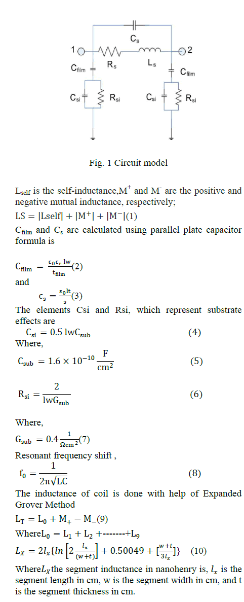
| Aim of this work is to design a bio-compatible sensor with maximum resonance frequency shift. Resonator consists of metal layers (Au) that make up the spiral coil structure and the insulator layers (Si3N4) that isolate the metal layer and the substrate (Si).The circuit model shown in fig.1, LS is the inductance of the spiral coil ;Cfilm is the capacitance of the dielectric thin film between the coil and the substrate ; CSi is the capacitance from the coil trace to the substrate for a half turn; CS is the capacitance between adjacent coil segments; RSi is the resistance of the substrate; and RS is the resistance of the spiral coil. |
 |
 |
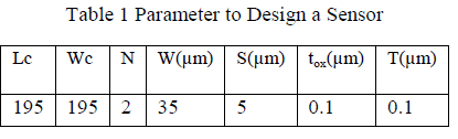
| C. Design of Sensor in Suspended Architecture In this paper, the effects of suspended architecture on a resonator for RF MEMS bio-implant sensors, which rely on resonance frequency shift to monitor fracture healing. Using a silicon substrate to fabricate sensor design, the suspended architecture obtained by etching the silicon through a carefully designed mask. This new design, which is obtained by partially removing the substrate of the single planar device, is called the single suspended device. Applying load to both of these device, and then observed their resonance frequencies, change in their resonance frequencies. Fig1 providesa top view of the architecture. An n-type 500 μm thick substrate with a <1 0 0> orientation.Silicon as an ideal substrate material for MEMS. Silicon (Si) is the most abundant material on earth. It almost always exists in compounds with other elements. Single crystal silicon is the most widely used substrate material for MEMS and Microsystems. The popularity of silicon for such application is primarily for the following reasons: It is mechanically stable and it is feasible to be integrated into electronics on the same substrate (it is a semiconducting material). Electronics for signal transduction such as the p or n-type piezoresistive can be readily integrated with the Si substrate-ideal for transistors. It has a melting point at 14000c, which is about twice higher than that of aluminum. This high melting point makes silicon dimensionally stable even at elevated temperature. Its thermal expansion coefficient is about 8 times smaller than that of steel, and is more than 10 times smaller than that of aluminum. GaAs is a compound semiconductor with equal number of Ga and As atoms. Because it is a compound, it is more difficult to process. It is excellent material for monolithic integration of electronic and photonic devices on a single substrate. The reason for being excellent material for photo electronics is its high electron mobility (7 times more mobile than silicon).GaAs is also a good thermal insulator. Low yield strength (only 1/3 of that of silicon) – âÃâ¬Ãâ¢badâÃâ¬Ãâ. The reason that the silicon is used as substrate instead of gallium arsenide is because of it is bio compatibility. We deposit a Si3N4 thin film using a plasma-enhanced chemical vapor deposition (PECVD) system; this film is 0.1 lm thick. We then lay down the first metal layer (contact layer) made of Au with a thickness of 0.1 μm. A 0.1 μm thick Si3N4 thin film is subsequently deposited. This film is patterned and vertical interconnection areas are opened using a wet etching process with HF. We also perform an Au (gold) metallization step to make the interconnects and top coil construction parameters to design a coil is shown in table.1 . Finally, using potassium hydroxide (KOH), we partially etch the silicon as shown in Fig.2. As a result of the etching of the substrate, the strain propagation will be higher. Since the strain first occurs in the substrate then pass to the dielectric and metal layers, with an etched substrate, there will be more strain and as a result, there will be more capacitance change. Hence, there will be a higher f0 shift which relies on resonance frequency shift to monitor fracture healing. |
 |
IV EXPRIMENTAL ANALYSIS |
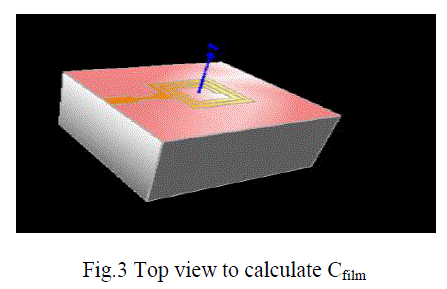
| To calculate LC of spiral coil the another fabrication step is performed is as shown in Fig 3 the process steps are as follows the first step in the fabrication procedure includes standard lithography and liftoff directly on a Si substrate to lay down the first metal layer made of Au with a thickness of 0.1 m. We then deposit a Si3N4 thin film using a plasma-enhanced chemical vapour deposition (PECVD) system; this film is 0.1 m thick. To pattern the Si3N4 film, we perform a second lithography to open vertical interconnection areas using a wet etching process with HF (hydrofluoric acid). In the subsequent Au metallization step, we erect the interconnection layer. In the third lithography and Au metallization steps, we construct the top coil and contact pads and finally obtain our on-chip microwave resonator. Figure 4. We characterize these fabricated devices using IntelliFab software. Then the results were used to calculate the resonance frequencyf0 results from the change in the capacitance of the film between the metal and substrate because of the modified area with the applied force. Where, Cfilm is the capacitance between the coil and the substrate.To calculate LC of spiral coil the another fabrication step is performed is as shown in Fig 3.4 the term LC that were used to calculate the resonance frequencyf0 results from the change in the capacitance of the film between the metal and substrate because of the modified area with the applied force. Where, Cfilm is the capacitance between the coil and the substrate. |
 |
| On applying the load to the sensor, it deforms (strains) under the applied stress. As the tissues mineralize strain decreases (due to the temporal shift in the load distribution) and modifies the operating frequency, thus allowing for observation of the process in the fracture. |
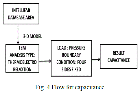 |
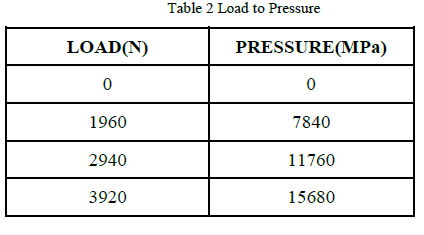
| Input is physical load (F), in the simulation applying force to the sensor is not possible, so first convert the force into pressure value as shown in table 2 |
P=F/A |
 |
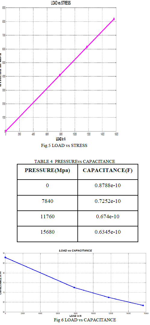
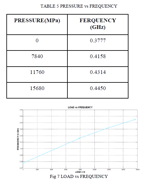
| Then we perform the Thermo Electro Mechanical analysis. Open the 3-D model in the TEM analysis for 3- D simulation then choose the analysis type as thermoelectromechanical relaxation, define the material property, fix boundary conditions and apply force to get the capacitance result. When applying the force the maximum stress in the material is taken out as reading and plotted as shown in Fig 5 Fig 7 showsthe increase in resonance frequency with appliedload. The reason is that, under load, the dielectric area decreases and the capacitance decreases. Hence, there is a concomitant resonance frequency increase. Fig 5 and 6 shows that When the plate is implanted, it assumes a majority of the load and demonstrates a relatively high associated strain. During the course of healing, the tissue consolidates and the strain in the plates decreases |
 |
 |
 |
V .CONCLUSION |
| In this work, the RF-MEMS bio strain sensors in suspended architecture with higher resonance frequency shift is designed and the maximum resonance frequency shift is obtained. The device fabricated is in the form of parallel plate capacitor(metal layer and the substrate) the silicon Nitrate plays the role as dielectric. The f0 shift results primarily from the change in the capacitance between substrate and metal layer. we conclude that it is possible to measure the change in the strain and hence to assess the healing process by means of this operating frequency shift. From the graph we infer thatthe increase in resonance frequency with appliedload. The underlying reason is that, under load, the dielectric area decreases and the capacitance decreases. Hence, there is increase in resonance frequency. |
References |
|