International Journal of Innovative Research in Science, Engineering and Technology
ISSN ONLINE(2319-8753)PRINT(2347-6710)
ISSN ONLINE(2319-8753)PRINT(2347-6710)
M.Ram kumar1, I.Sayed mohammed 2 , J.Manikanda prashath3
|
| Related article at Pubmed, Scholar Google |
Visit for more related articles at International Journal of Innovative Research in Science, Engineering and Technology
Within the photovoltaic power-generation market, the ac PV module has shown obvious growth. This paper proposes an implementation of Single Ended Primary Inductor (SEPIC) converter and cascaded multi level inverter for an AC load using Photovoltaic energy as a source. This paper proposes a converter that employs a continuousconduction- mode SEPIC converter with low reverse-recovery loss. To convert the boosted DC output voltage from PV module into AC, a cascaded multi level inverter with multi carrier pulse width modulation is implemented. An operation principle and a detailed analysis of the proposed converter are presented. A 12V input voltage, (220-230)V output voltage of the proposed converter has been implemented. The simulation work of these SEPIC converter and cascaded multi level inverter fed RL load have been done using MATLAB software
Keywords |
| PV cell, SEPIC converter, cascade multilevel inverter, multi carrier PWM |
INTRODUCTION |
| Thephotovoltaic energy system has the advantages of absence of fuel cost, no environmental impacts, low maintenance and lack of noise and also it is a kind of renewable energy system. So it is becoming popular in the recent years, as a resource of energy. Modelling and simulation of PV array based on circuit model and a mathematical equation is proposed [9]. As the photovoltaic (PV) cell exhibits the nonlinear behaviour, while matching the load to the photovoltaic modules, DC-DC power converters are needed. There are several converter configurations such as Buck, Boost, Buck-Boost, SEPIC, ̉̉ UK, Fly-back, etc. Buck and Boost configurations can decrease and increase the output voltages respectively, while the others can do both functions. Buck, Boost, Buck Boost converters as interface circuits are proposed and analyzed in [6]. CUK and SEPIC converters are analyzed in [1,7].the SEPIC converter should operate with high switching frequency. However, as the switching frequency increases, the reverse recovery current of the output diode affects the switching devices in the form of additional switching losses. Other adverse effects of the reverse-recovery problem include electromagnetic interference (EMI) noises and additional thermal management. Also, the switch utilisation factor in the SEPIC converter is much lower than that of other topologies, such as the buck and boost converters. In other words, the power-handling capabilities of the semiconductor devices in the SEPIC converter are much lower than those of the buck or the boost converter at the same power level. Thus, the reduction of reverserecovery loss is particularly important for the SEPIC converter. |
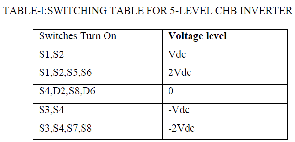
| Different topologies MLIs for the conversion from DC to AC are available such as Neutral point clamped MLI (NPC-MLI), Flying capacitor MLI (FC-MLI), Cascade H-Bridge MLI (CHB-MLI) and Asymmetrical Cascade HBridge Multilevel inverters. Among them CHB-MLIs are mostly used for PV applications because each cell of CHBMLI requires separate DC sources which can be easily supplied by individual PV arrays and each H-Bridge cell will be available in a single module6. The number of levels of the output wave form increased by cascading the no. of HBridge cells. There is a large no. of control techniques developed so far to control the operation of multilevel inverters such as SVPWM, SPWM, OHPWM, SHE-PWM, Hybrid modulation. |
| In these techniques SPWM is the easy to increase the number of levels in the output waveform with lower harmonic content. In SPWM control technique the gate pulses generated by comparing the sinusoidal reference waveform with the Triangular carrier waveforms. This paper presents the simulation results of a 5-level CHB-MLI with multi carrier PWM control techniques for PV applications. The function of an inverter is to change a dc input voltage to a symmetric |
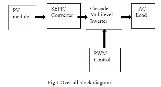
| AC output voltage of desired magnitude and frequency. To drive the AC load, the output dc voltage of SEPIC converter is converted into AC by means ofcascade multilevel inverter.In this paper PV source fed AC load is proposed with SEPIC converter and cascade multilevel inverter as interface circuits. Multi carrier pulse width modulation technique is employed for the control of cascade multilevel inverter. The overall block diagram is shown in Fig.1 |
 |
II. ANALYSIS OF SEPIC CONVERTER AND PV CELL |
| PV system directly converts sunlight into electricity. The basic device of a PV system is the PV cell. Cells may be gathered to form modules or arrays. More sophisticated applications require DC-DC converters to process the electricity from the PV device. These converters may be used to either increase or decrease the PV system voltage at the load. The proposed SEPIC converter operates in boost mode. |
| A. PV Module Characteristics: |
| The practical equivalent circuit of a PV module is shown in Fig.2 |
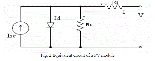 |
| In the equivalent circuit, the current source represents the current generated by light photons and its output is constant under constant temperature and constant irradiance. The diode shunted with the current source determines the I-V characteristics of PV module. There is a series of resistance in a current path through the semiconductor material, the metal grid, contacts, and a current collecting bus. These resistive losses are lumped together as a series resistor (Rs). Its effect becomes very noteworthy in a PV module. |
| The loss associated with a small leakage of current through a resistive path in parallel with the intrinsic device is represented by a parallel resistor (Rp). Its effect is much less noteworthy in a PV module compared to the series resistance, and it will only become noticeable when a number of PV modules are connected in parallel for a larger system. The characteristic equation which represents the I-V characteristic of a practical photovoltaic module is given below |
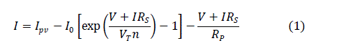 |
| Where I and V are the PV cell current and voltage respectively, IPV is the photovoltaic current, Io is the reverse saturation current of diode, Vt= Ns*kT/q is the thermal voltage of the array with Ns cells connected in series, k is the Boltzmann constant (1.3806*10-23J/K), T is the temperature of the p-n junction, q is the electron charge and n is the diode is constant. ïÿýïÿýïÿýïÿýïÿýïÿýandïÿýïÿýïÿýïÿý are given as follows |
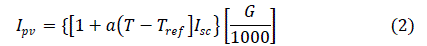 |
| Where “a” is temperature coefficient of ïÿýïÿýïÿýïÿýïÿýïÿý , G is the given irradiance in W/m2 and Egis the band gap energy (1.16eV for Si) |
A. Design of SEPIC Converter: |
1) Introduction: |
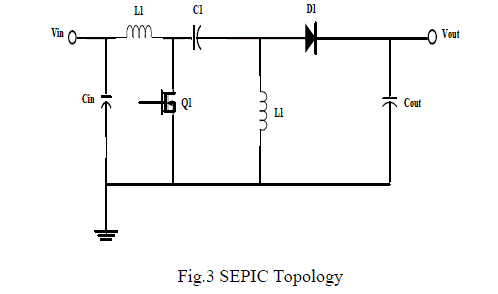
| Using a coupled inductor takes up less space on the PCB and tends to be lower cost than two separate inductors. The capacitor Cs isolates the input from the output and provides protection against a shorted load. |
 |
 |
2) Duty Cycle Consideration: |
| For a SEPIC converter operating in a continuous conduction mode(CCM),the duty cycle is given by: |
 |
 |
| A capacitor that meets the RMS current requirement would mostly produce small ripple voltage on ïÿýïÿýïÿýïÿý.Hence, the peak voltage is typically close to the input voltage. |
7) Output Capacitor Selection: |
| In a SEPIC converter, when the power switch Q1 is turned on, the inductor is charging and the output current is supplied by the output capacitor. As a result, the output capacitor sees large ripple currents. Thus the selected output capacitor must be capable of handling the maximum RMS current. The RMS Current in the output capacitor is: |
 |
III. SIMULATION RESULTS FOR SEPIC CONVERTER |
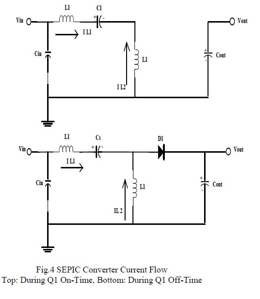
| This converter Fig. 5 has two inductors and two capacitors. The capacitor C1 provides the isolation between input and output. The SEPIC converter exchanges energy between the capacitors and inductors in order to convert the voltage from one level to another. The amount of energy exchanged is controlled by switch, which is typically a transistor such as a MOSFET. |
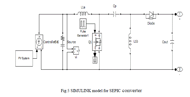
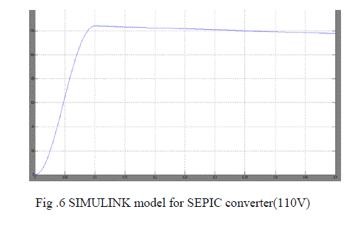
| The MATLAB simulation model of SEPIC output voltage waveform is shown in Fig. 6. |
 |
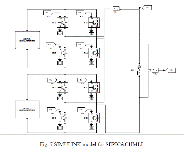
| In this topology, each cell has separate dc link capacitor and the voltage across the capacitor might differ among the cells. So, each power circuit needs just one dc voltage source. The number of dc link capacitors is proportional to the number of phase voltage levels .Each H-bridge cell may have positive, negative or zero voltage.Final output voltage is the sum of all H-bridge cell voltages and is symmetric with respect to neutral point, so the number of voltage levels is five. Cascaded H-bridge five level inverters typically use IGBT switches. These switches have low block voltage and high switching frequency.The MATLAB simulation model of SEPIC converter and CHMLI fed RL load is shown in Fig .7 |
 |
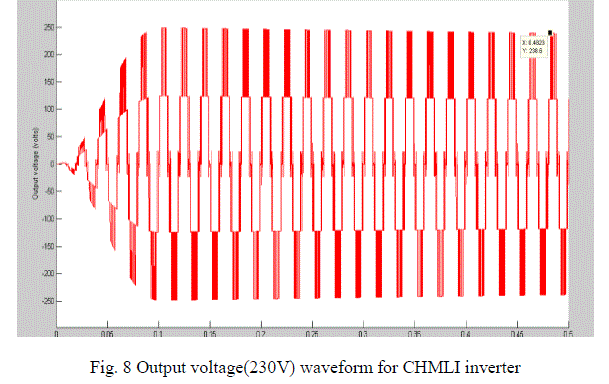
| The SEPIC converter output is a boosted DC voltage of PV module output. The output of the SEPIC converter is fed to the cascade multi level inverter . The magnitude of the output voltage of the inverter is controlled by the amplitude of the reference sine wave and hence the amplitude modulation index. The frequency of the inverter output voltage is controlled by the frequency of the reference signal. The current output of the inverter is dependent on the load impedance. The controlledmagnitude and frequency of the inverter output voltage is(220-230v)given to AC load. Finally the voltage of the AC load is measured for the given irradiance and temperature. |
 |
 |
IV. CONCLUSION |
| This paper presented the simulation work of a Photovoltaic array feeding a RL load. SEPIC converter and cascade 5 level inverter were used as interface between PV module and the RL load. The voltage level of the PV panel is improved using SEPIC converter &cascade h-bridge multilevel inverter. The simulation works of these circuits were carried out in the MATLAB software. The proposed SEPIC&CHMLI inverter is to reduce both voltage & current THD of the inverter. The 230v output voltage is obtained with above proposed topology in simulation. The boosted DC voltage of the SEPIC converter circuit output and inverted AC output waveforms were shown in the results. |
References |
|