International Journal of Innovative Research in Science, Engineering and Technology
ISSN ONLINE(2319-8753)PRINT(2347-6710)
ISSN ONLINE(2319-8753)PRINT(2347-6710)
Rajni Sharma 1, Sanjay Chopade 2
|
| Related article at Pubmed, Scholar Google |
Visit for more related articles at International Journal of Innovative Research in Science, Engineering and Technology
SRAM area is expected to exceed 90% of overall chip area because of the demand for higher performance, lower power, and higher integration. To increase memory density, memory bitcells are scaled to reduce their area by 50% each technology node. High density SRAM bitcells use the smallest devices in a technology, making SRAM more vulnerable for variations. This variation effect the stability of SRAM. This paper investigates Static random access memory (SRAM) stability in hold/standby, read and write mode. In this paper different techniques to find Static Noise Margin (SNM), Read margin and write margin are discussed. The effect of supply voltage, transistor scaling, word line voltage, threshold voltage, and temperature on SRAM stability is analysis in Standby and Read Mode. From 0.7V to 1.2V the read stability increase 231% and Standby stability increase 135%. When the cell ratio changes from 1 to 3 the stability of SRAM during read mode gets doubled. This paper also investigate the Data Retention Voltage(DRV) during standby and read mode which is the minimum voltage required to hold or read data, any voltage below DRV can flip the state of SRAM. The DRV 6T SRAM in Standby mode is 0.14V and that in read mode is 0.29V.
Keywords |
| Static Random Access Memory (SRAM), Static Noise Margin (SNM), Cell Ratio (CR), Pull up Ratio (PR). |
INTRODUCTION |
| Static Random Access Memories (SRAMs) continue to be important components across a wide range of microelectronics applications from consumer wireless to high performance server processors, System on Chip (SoC) and multimedia applications. Improvement in performance and cost of integrated circuit (IC) has been achieved largely by transistor scaling (i.e., minimum feature size reduction by a factor of 0.7 in every new technology node, or every 2 years) as defined by Moore’s Law [1]. The resultant exponential growth in device count per chip has been led by the miniaturization of the static-random-access-memory (SRAM) bit-cell [2]. Frequently used in integrated system, SRAM cell has a minimum foot print to achieve high integration density consistent with the reliability and performance required [3]. In particular, continued SRAM cell-area scaling for increased storage density, reduction in Supply voltage (VDD) for lower stand-by power consumption, and enhanced yield necessary to realize larger-capacity SRAM arrays become increasingly difficult to achieve either by reducing the number of transistor use to design SRAM or by reducing the size of transistor [4]. |
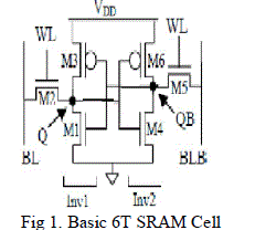
| Two aspects are important for SRAM cell design: the cell area and the stability of the cell. The cell area determines about two-thirds of the total chip area. The cell stability determines the soft-error rate and the sensitivity of the memory to process tolerances and operating conditions. The two aspects are interdependent since designing a cell for improved stability invariably requires a larger cell area. The stability as expressed by the static-noise margin has been investigated for CMOS SRAM cell has been analysis by J. Lohstroh [5], K.Anami[6] and F.J.List I 1986[7]. However, these studies have been limited to computer simulations; analytic work has not yet been reported. In 1987 E.Sevinch[10] found the SNM of SRAM cells both from an analytic as well as a simulation point of view, in the context of submicrometer MOS technology. In this work a graphical method to find SNM before that butterfly curve was found to measure the SNM. In 2006, Evelyn Grossar [11] found a new method to find stability that was the N curve which proved to be more accurate for finding write and read stability. In 2008, Zheng guo [12] found five methods to calculate write stability and the method for read stability. For high speed application the power has to be reduced and stability has to increase. So the effect of process, supply voltage and temperature was studies on SRAM [14]. Transistor scaling and word line voltage modulation also effect stability was found by Benton H. Calhoun [16]. The Fig.1 demonstrates the classic six-transistor cell formation used for CMOS static random-access memories (SRAM). The cell comprises two cross-coupled CMOS inverters that are used to accumulate one bit of information, and two N-type transistors(M2.M5), known access transistor are connected to the word line (WL) to perform access read and write operation thought the bit lines (BL and BLB). The stability of SRAM reduces with reduction in transistor size, so this paper analyse the effect of transistor scaling, Supply voltage and temperature (PVT) on stability. Not only that but this paper includes the effect of transistor scaling and word line voltage on SRAM stability during standby/hold mode and read mode. This paper uses a 32nm PTM file. So the stability can improve without increasing the power consumption and cell area. |
| The remaining paper is organized as follow Section II discuss briefly about working and failure mechanism of 6T SRAM whereas section III present a detail about cell stability and parameter affecting stability are discussed in detail in section IV. Finally section V draws the conclusion. |
 |
6T SRAM WORKING AND FAILURE MECHANISM |
| A. 6T SRAM Working |
| The SRAM cell operates in three basic modes that are Standby, Read and write mode [8]. In Standby mode the SRAM cell is able to hold the data indefinitely as long as it is powered. So during standby mode the word line is grounded. In read mode the bit-lines are usually pre-charged to a high level (VDD) and then the word-line is selected (pulsed to a high level). On the side of the cell storing a logical ‘0’ (i.e., a low voltage), the bit-line is discharged via the access transistor and pull-down transistor, so that a differential voltage develops between the bit-lines [9]. This differential voltage should be large enough for a sense amplifier to detect the state of the cell. The differential voltage must not be too large, however; otherwise the cross-coupled inverters could flip their state. (The read operation should be non-destructive). Boundary condition on M1 and M2 sizing to avoid read upset is achieved by equating discharging Current through M1 and M2 as given in equation 1[10].The cell ratio, which is the ratio of the strength(drive current) of the pull-down transistor to that of the access transistor, should be sufficiently large to ensure that such a read disturbance does not occur. |
 |
| This simplifies to |
 |
| Where CR is called Cell Ratio or β ratio defined as, |
| Cell Ratio (CR) = (W1/L1) / (W2/L2) |
| For a write operation, the bit-lines are driven to complementary voltage levels via a write driver and then the word-line is selected. On the side of the cell for which the bit-line voltage is logical ‘0’ (i.e., a low voltage), the internal storage node is discharged through the access transistor [6]. The cross-coupled inverters raise the voltage on the opposite storage node and latch the cell. The discharging strength of the access transistor must overcome the restoring strength of the pull-up transistor. The pull up ratio, which is the ratio of the strength of the pass-gate transistor to that of the pull-up transistor should be sufficiently large to ensure that write failure does not occur. Sizing constraint on PMOS and access transistor to avoid write failure is obtained by equating current passing through M4 and M5 as given below in equation 2 [15]. |
 |
| Where PR is called Pull up Ratio or α Ratio defined as, |
| Pull up Ratio (PR) = (W4/L4) / (W5/L5) |
| B. Failure Mechanisms |
| While designing SRAM we should take care of the above design criteria along with various SRAM cell parametric so that failure due to read, write access and hold does not occur [16]. |
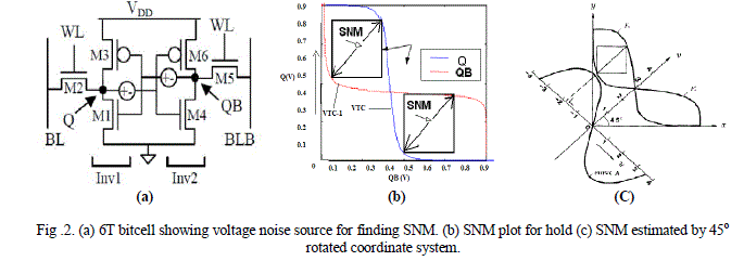
| Read Failure – This failure occurs while reading the content of an SRAM cell. Assume that node Q in Fig. 1 is storing a “0” and BL is discharging through M2 and M1. If the resistance of pull-down transistor M1 is higher than that of access transistor M2, a voltage ripple VQ is developed due to resistive divider formed by M1 and M2 [10]. If VQ exceeds the switching threshold of the inverter formed by M6 and M4, the cell state flips while reading. The read failure can be reduced by increasing the difference between the voltage rise at the node storing “0” and the trip-point of the inverter associated with the node storing “1” [14 ]. |
| Write Failure – It is an unsuccessful write to the SRAM cell. Write failure occurs if the node storing “1” cannot be discharged through the access transistors during the word line turn on time. The write failure can be reduced by increasing the word line turn on time with write access time increased, which unfortunately makes SRAM slower [11]. |
| Access Failure – Access failure occurs if the voltage difference between the two-bitlines at the time of sense amplifier firing remains below the offset voltage of the sense amplifier. Access failure occurs due to the reduction of the bit-line discharging current through the pass transistor and pull-down transistor. Clearly, a faster bitline discharge can be achieved by reducing the resistance in the discharge path by making the pull-down transistor stronger. However, such improvements come at the price of larger cell area which is not recommended for high density SRAMs [13]. |
| Hold Failure - The hold failure occurs due to high-leakage of the pull-down NMOS transistors connected to the node storing “1”. In scaled technology, at lower supply voltage (VDD), due to high leakage of the pull-down transistor, the node storing “1” reduces from VDD. If that voltage becomes lower than the trip-point of the inverter storing “0” the cell flips in the hold mode. This failure can be avoided by reducing leakage in standby mode using high-VT pull-down transistors. This improvement comes at the price of read delay. |
6T SRAM STABILITY |
| To improve the performance of SRAM in nano scaled technology there is a need to investigate stability of SRAM in all three modes of operation. The stability of SRAM during hold/standby mode can be measure by static noise margin (SNM).First the methods to calculate SNM is discussed in this section, the later part of the section will consider methods to measure read and write stability which is also known as read and write margin. |
| A. Static Noise Margin (SNM) |
| The static noise margin of SRAM is defined as the minimum DC noise voltage necessary to flip the state of cell. Fig 1(a) shows the placement of noise source in 6T (transistor) bitcell schematic to measure the SNM. This method is called the trail ad error method and we have to change the value of noise source again and again, by checking the voltage at which the inverter flips the state. The second method is known as graphical method, in this method the VTC (Voltage transfer curve) of two inverters are plotted with one inverse as shown in fig 1(b) and finding the maximum size of square that can fit in the curve. The side of the square gives the value of SNM or we can measure the length of diagonal and divide it by square root of 2. There are different test setup to plot this curve, which is also known as butterfly curve. The best graphical method to calculate SNM is given by Seevinch [10]. This method is used to calculate SNM in this paper, in this technique the output of inverter is shifted to other axis which is 45° rotated and then the SNM is found by subtracting the value of two curve form and taking the maximum value and dividing it by square root of two. Fig 2(c) shows the common graphical representation of SNM. |
 |
| B. Read Stability. |
| The read stability of SRAM can be obtained in three ways first is by plotting the SNM curve as discuss above for read mode. The stability is usually defined by the SNM as the maximum value of DC noise voltage that can be tolerated by the SRAM cell without changing the stored bit. The third one is plotting the n curve, for extracting the N-curve during read operation, the bit-lines are clamped at VDD the word-line is activated. Next, a voltage sweep Vsweep from 0 V to VDD is applied at “0” internal storage node Q/QB to obtain the corresponding current I at that node . The third method for measuring the read stability of SRAM cell in large array is, BL current at the ‘0’ storage node is monitored while ramping down the cell supply with the bit line pre charged WL driven by nominal supply. The difference between the nominal supply and the cell supply causing current to drop gives the read stability. In this paper the SNM method to find the cell read stability (RSNM). |
| C. Write Stability. |
| There are already five exiting static approach to measure write stability. During a write operation, a low going bit line voltage pulls down the ‘1’ storage node as the word line is held high until the trip point of the inverter formed by the PMOS and NMOS is reached and the bit cell is successfully written[15]. |
| We have used the Bit line write margin (BLWM) to measure write stability. This is the maximum bit line voltage able to flip the cell state and can be measured through monitoring the BL current at the ‘0’ storage node while ramping down the other bit line voltage with word line held high. The voltage at the other bit line that induces a sudden drop in current in the bit line is the write margin as shown in fig 3.The write stability is measured by this method is 650mV. |
 |
| We can also measure the write stability by word line write margin (WLWM), it can be defined as the maximum of (VDD – VWL ) in a word line voltage sweep node. The ways are N curve, SNM and to measure the writeable current IW. Table 1.below give the stability of SRAM during stand by, read and write mode |
 |
RESULT AND DISCUSSION |
| Data retention of the SRAM cell, both in standby mode and during a read access, is an important functional constraint in advanced technology nodes. The cell becomes less stable with lower supply voltage, increasing leakage currents and increasing variability, all resulting from technology scaling. |
| A. Data Retention Voltage (DRV) |
| Data Retention Voltage (Vdr): Min. power supply voltage to retain high node data in the standby mode. There are two nodes (q and qb) of the SRAM cell for storing value either 0 or 1[16]. Then decrease the power supply voltage until the flip the state of SRAM cell or content of the SRAM cell remain constant. VDD scales down to DRV, the Voltage Transfer Curves (VTC) of the internal inverters degrade to such a level that Static Noise Margin (SNM) of the SRAM cell reduces to zero. |
| If Q=1, Q’=0, it is changes the value of Q=0, Q’=1 after decreasing the value of the power supply voltage. Data retention voltage should be less than threshold voltage. The DRV for Standby mode is 0.14V and for Read mode is 0.29V any voltage below this value in standby/read mode can cause SRAM to flip state. |
| B. Effect of transistor sizing. |
| We establish a metric to quantify the SNM improvement during read operations considering transistor width modulation defining the following ratios: |
| Cell Ratio (CR or β) = (WNMOS) / (WACCESS) |
| Pull up Ratio (PR or α) = (WPMOS) / (WACCESS) |
| Where WACCESS= β*Wmin, and Wmin is the minimum transistor width allowed by the technology. To keep cell area within reasonable values, we restrict the values of α and β ratios between the minimum, 1, and a maximum of 2.5, (i.e. αmax = βmax = 2.5). |
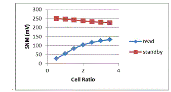
| Fig. 4 plots the SNM improvements using the transistor width modulation technique during read operations and decreases during standby mode. The values of SNM decrease by increasing the cell ratio. The decrease in SNM during standby mode is small as compared to the increase in read mode. We need to increase the stability of SRAM and so we prefer to go for cell ratio between 1 to 3. We have taken the reading for CR 0.5, 1, 1.5, 2, 2.5. We have chosen the value CR=2 for better results. Fig 4 Show the effect of cell ratio on SNM. When the cell ratio changes from 1 to 3 the stability of SRAM during read mode gets doubled. |
 |
| Pullup ratio does not have any major effect on SNM in stand by and read mode. Pull up ratio effect the BLWL. The value of BLWM decreases as pull up ratio increase. |
| C. Impact of Process variation, Supply Voltage and Temperature (PVT) |
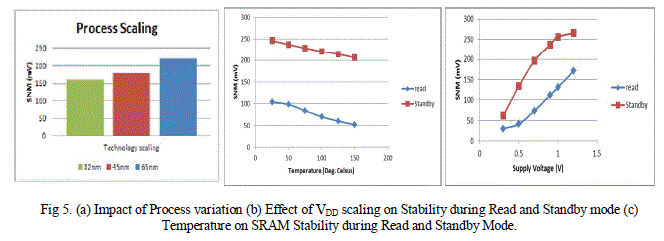
| Process scaling causes the SNM of SRAM bit cell to degrade. To understand the effect of process scaling we have used predictive technology models for 65nm, 45nm and 32nm.the typical SNM reduces with technology scaling and with supply voltage reduction. This means that it is difficult to make a robust array in a scaled technology and that lowering supply voltage to reduce power degrades [18].Fig 5(a). Shows the impact of process variation on stability of SRAM. As the supply voltage decrease the value of SNM also decrease. So, it is essential to maintain full VDD during read cycle and standby mode so that we get a better value of SNM. That means a better stability [12]. Fig 5(b) below shows the effect VDD on stability of SRAM for both read and standby mode. However a low value of VDD is always prefer in standby mode to reduce the power consumption. This technique is widely adopted in nanometer technologies for which leakage has increase dramatically. From 0.7V to 1.2V the read stability increase 231% and Standby stability increase 135%. |
| Although temperature may have a significant impact on other design parameters like access time, it has relatively small effect on SNM analysis [17]. The SNM during standby mode and read mode reduces, due to increases in temperature. The reduction in SNM is small in comparison of decrease in RSNM during read mode. But as stability in read and standby mode is important we will go for temperature between 25 to 50°C. Fig 5(C) shows temperature on stability (SNM) during read and standby mode. We have taken temperature 25°C for all other readings. As the temperature increases for 25 to 150 the Stability during read mode reduces 50% whereas the stability in Standby mode decreases by 16.66%. |
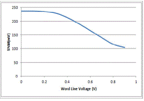 |
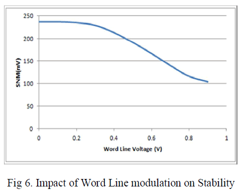
| D. Impact of Word line voltage modulation |
| The word-line voltage modulation is another alternative to increase the cell stability at low power supply levels compatible with recommended cell layout (α≈β≈1). This approach is based on reducing the maximum voltage swing of the word-line to maintain the cell access transistor weakly-saturated during the read operations. Fig. 6 plots the relationship between the SNM and the word-line voltage. |
| The word-line voltage controls the SRAM cell access state and allows two modes: hold and access operations (read and write)[19]. As shown in Fig. 6, the SNM could be improved by reducing the word-line voltage during read operations with respect to VDD (world-line voltage will not be reduced during write mode). This technique may allow a substantial improvement of the SNM during read without requiring any modification of the SRAM cell array design. |
 |
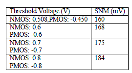
| E. Impact of Threshold voltage variation |
| In this paper we can also going to see the effect of threshold voltage on stability of SRAM during standby and read mode. The stability of SRAM increases with increase in its threshold voltage. We have change the value of threshold voltage from0.35 to 0.65 and seen its effect on Vth (threshold voltage). We can improve the stability of both SNM and RSNM by increasing the threshold voltage [20].The table below specify the value of SNM and RSNM at different threshold voltage. |
 |
CONCLUSION |
| In this paper, the working and failure mechanism of 6T SRAM design by using CMOS file at 32 nm technology is studied. This paper reviews different methods to find the Stability of SRAM in standby, read and write mode of 6T SRAM design. In the paper the impact of PVT (Process, Supply Voltage and Temperature), cell ratio, word line voltage, and threshold voltage on stability during read and standby mode is analyse. This paper shows why stability is important as technology scales down, as the Stability decrease as process technology node decreases. As the supply voltage increase from 0.7V to 1.2V the read stability increase 231% and Standby stability increase 135%, but we can’t increase the supply voltage considering the power consumption. When the cell ratio changes from 1 to 3 the stability of SRAM during read mode gets doubled, but increasing the cell ratio beyond a limit increases the cell area. So in this paper the value of CR is taken 2 for rest of the reading. The pull up ratio has little or no effect on read and standby stability but it affects the write stability. As the pull up ratio increase the BLWL decrease, so it is necessary to keep the ratio as small as possible around 1. As the temperature increases for 25 to 150 the Stability during read mode reduces 50% whereas the stability in Standby mode decreases by 16.66%. So to increase stability it is necessary to keep temperature as minimum as possible, probably in between 25 to 50°C.Thershold voltage has impact on both RSNM and SNM equally, they both increases with increase in Vth. So the value of threshold voltage should be as high as possible. We have also seen the impact of word line voltage on SNM. We can reduce the word line voltage slightly to improve the RSNM. All the simulation work was done using Hspice. |
References |
|