


 21 / 60

Page 63
conferenceseries
.com
Volume 6
Research & Reviews: Journal of Material Sciences
ISSN: 2321-6212
Advanced Materials 2018
September 04-06, 2018
September 04-06, 2018 | Zürich, Switzerland
21
st
International Conference on
Advanced Materials & Nanotechnology
Growth control of vertical nano graphene network in plasma enhanced chemical vapor deposition
and its emerging applications
Keigo Takeda
1
, Takuya Suzuki
1
, Hitoshi Nozaki
1
, Mineo Hiramatsu
1
, Hiroki Kondo
2
and
Masaru Hori
2
1
Meijo University, Japan
2
Nagoya University, Japan
C
arbon nanowalls (CNWs) composed of few layer graphenes standing vertically on the substrate have a maze like structure
formed by a self-supporting network of wall structures. The 3-dimensional structure of CNWs would be useful as a
nano platform for electrochemical applications such as sensing, energy conversion, etc., because of the conductive carbon
structure with the large surface and the wide capability of surface modification including decoration with catalysts such as
metal nanoparticles. For achieving the CNWs applications to such fields, control of CNWs morphologies including interspace
between adjacent nano walls is crucial issue. In this study, we carried out the CNWs growth with plasma enhanced chemical
vapor deposition (PECVD) using CH
4
/H
2
/Ar mixture with emphasis on the surface morphology control of CNWs. The
CNWs were grown on a SiO2 film synthesized on a Si substrate by PECVD using inductively coupled CH
4
/H
2
/Ar plasma.
Moreover, emission intensities of CH species (wavelength: 430 nm) and H atom (Balmer α line, wavelength: 656 nm) in the
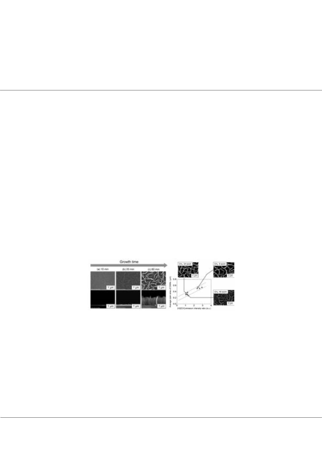
plasma were monitored by optical emission spectroscopy. To estimate the interspace between adjacent nanowalls, the average
area surrounded by nanowalls was evaluated from the top view observation of grown CNWs observed by scanning electron
microscope. From results, it is found that the behavior of average area change has a correlation with the [H]/[CH] emission
intensity ratio in the CVD plasma with Ar/CH
4
/H
2
mixture. It is considered that the balance between carbon precursors
and etching radicals in the CVD plasma affect the nucleation in the initial growth stage of CNWs, therefore, the interspaces
between adjacent walls changed as a function of the [H]/[CH] emission intensity which is relative density ratio of gas phase
radicals. In our presentation, we report the effects of ion bombardment and catalytic metals on the nucleation of nano walls to
achieve the control of space between adjacent walls.
Figure 1:
Average area surrounded by the grown nanowalls as a function of [H]/[CH] emission intensity ratio in the plasma
Biography
Keigo Takeda has completed his PhD at Nagoya University and Postdoctoral studies at Graduate School of Engineering, Nagoya University. He is an Associate Professor
at Meijo University since 2017. He has published more than 90 papers in reputed journals. His current research interests include Reaction mechanisms of reactive species
in plasma processes for advanced materials synthesis, Fine Processing Technology and Biomedical Applications, etc.
ktakeda@meijo-u.ac.jpKeigo Takeda et al., Res. Rev. J Mat. Sci. 2018, Volume 6
DOI: 10.4172/2321-6212-C3-020