


 4 / 18

Page 75
Notes:
conferenceseries
.com
RRJOMS | Volume 5 | Issue 4 | July, 2017
July 27-29, 2017 Vancouver, Canada
10
th
International Conference on
Emerging Materials and Nanotechnology
Number of layer dependent direct optical transition from monolayer to pentalayer in synthesized
large area MoSe
2
Jae-Hun Jeong, Yoon Ho Choi, Kwang Sik Jeong, Mann-ho Cho, Hanbom Park
and
Dasol Kim
Yonsei University, South Korea
T
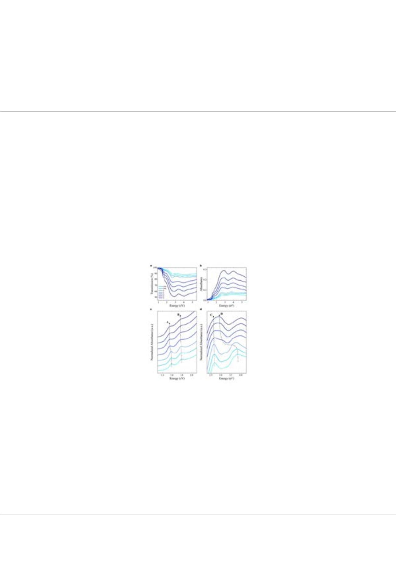
wo-dimensional transition metal dichalcogenides (TMDs) have attracted great interest for applications in optoelectronic
device. We studied the optical properties of the large area MoSe
2
thin film on c-axis sapphire (0001) substrate grown
by molecular beam epitaxy (MBE). Photoluminescence (PL), Raman, X-ray diffraction (XRD), and X-ray photoelectron
spectroscopy (XPS) were measured to evaluate the film quality. We obtained the optical absorption spectra of mono-, bi- and
tri-layer MoSe
2
and observed optical critical point which is corresponded to the direct transition at Г-point of the Brillouin
zone (BZ) at ~3 eV. Increasing the number of layer, the intensity of the absorption peak at Г-point was increased and its
position was shifted. The changes in peak at Г-point are caused by the band structure depending on the number of layer,
resulting in the modulation of the joint density of state (JDOS). Since the geometrical band shape of conduction band and
valance band are similar around Г-point for few layer MoSe
2
, both Van Hove singularities (VHS) and band nesting contribute
to strong absorption peak. Using 3eV optical pump, we can selectively excite the MoSe
2
by choosing suitable number of layers.
The modulation of band structure and strong photon-electron interaction of 2D material would be widely applied to photonic
and optoelectronic devices.
Biography
Jae-Hun Jeong has expertise in the properties of two-dimensional materials such as MoS2 and MoSe2. His large-area growth technology and in-depth research
have laid the foundation for 2D materials to be used in next-generation applications. His research approach, which focuses on deep physics and his large-area
growth techniques are expected to make a valuable contribution to the development of new-level devices
duanjjh@gmail.comJae-Hun Jeong et al., Res. Rev. J Mat. Sci. 2017
DOI: 10.4172/2321-6212-C1-003