


 5 / 18

Page 76
Notes:
conferenceseries
.com
RRJOMS | Volume 5 | Issue 4 | July, 2017
July 27-29, 2017 Vancouver, Canada
10
th
International Conference on
Emerging Materials and Nanotechnology
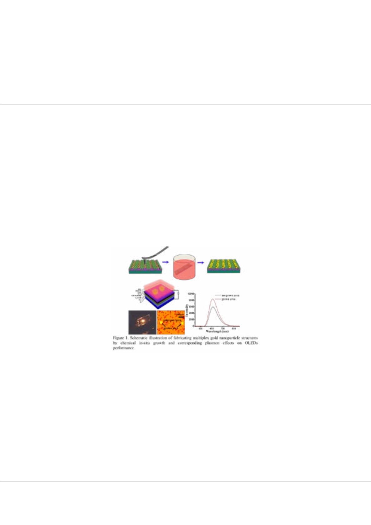
Fabrication of multiplexed plasmonic nanoparticle structures based on AFM lithography
Jianmei Chen
Soochow University, China
P
recisely positioning of plasmonic nanoparticles intomultiplexednanostructureswithhigh controllability and reproducibility
plays an important role for emerging advanced device applications. Many techniques employed to produce multiplexed
nanostructures are limited by complicate fabrication process and difficulties with scalability. Here the work reports a scalable
strategy to fabricate multiplexed plasmonic nanoparticle structures by mechanical scratching with AFM lithography. Under the
assistance of polymer resist, gold nanoparticles assembled on the silicon substrate can be directly scratched by AFM tip to form
well defined nanostructures, and different size or shape of gold nanoparticles can be controllably scratched at a high speed of
1000 µm/s and remain the same integrity of particle arrays after removing the polymer. By precisely controlling the scratching
loading force, multiplexed nanostructures of plasmonic nanoparticles can be further achieved which demonstrate multiplex
plasmonic properties and surface-enhanced Raman scattering (SERS) responses. When the multiplexed nanostructure is
further integrated into organic light-emitting diodes device, it intuitionisticly expresses multiplexed plasmonic effects on
the device performance. It gives a new aspect for multilevel assembly to the application of multiplexed SERS response or
exploration for the plasmon enhanced devices.
Biography
Jianmei Chen received her BEng in Chemical Engineering and Materials Science from Shandong Normal University, Shandong, China, in 2011. She received her
PhD degree in Material Science and Engineering from Institute of Functional Nano and Soft Materials (FUNSOM), Soochow University, Jiangsu, China, in 2017.
She mainly focuses on the AFM lithography technique and application of Kelvin probe microscope in charge storage in dielectric material, plasmonic nanostructures
fabrication and application in optoelectronics
chenjianmei90@sina,cn
Jianmei Chen, Res. Rev. J Mat. Sci. 2017
DOI: 10.4172/2321-6212-C1-003